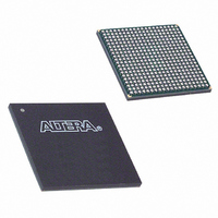
EP1C20F400C6N Altera, EP1C20F400C6N Datasheet - Page 36

EP1C20F400C6N
Manufacturer Part Number
EP1C20F400C6N
Description
IC CYCLONE FPGA 20K LE 400-FBGA
Manufacturer
Altera
Series
Cyclone®r
Datasheet
1.EP1C3T144C8.pdf
(106 pages)
Specifications of EP1C20F400C6N
Number Of Logic Elements/cells
20060
Number Of Labs/clbs
2006
Total Ram Bits
294912
Number Of I /o
301
Voltage - Supply
1.425 V ~ 1.575 V
Mounting Type
Surface Mount
Operating Temperature
0°C ~ 85°C
Package / Case
400-FBGA
Family Name
Cyclone®
Number Of Logic Blocks/elements
20060
# I/os (max)
301
Frequency (max)
405.2MHz
Process Technology
0.13um (CMOS)
Operating Supply Voltage (typ)
1.5V
Logic Cells
20060
Ram Bits
294912
Operating Supply Voltage (min)
1.425V
Operating Supply Voltage (max)
1.575V
Operating Temp Range
0C to 85C
Operating Temperature Classification
Commercial
Mounting
Surface Mount
Pin Count
400
Package Type
FBGA
Lead Free Status / RoHS Status
Lead free / RoHS Compliant
Number Of Gates
-
Lead Free Status / Rohs Status
Compliant
Other names
544-1687
Available stocks
Company
Part Number
Manufacturer
Quantity
Price
Company:
Part Number:
EP1C20F400C6N
Manufacturer:
ALTERA
Quantity:
237
Cyclone Device Handbook, Volume 1
Figure 2–22. Global Clock Generation
Notes to
(1)
(2)
(3)
2–30
Preliminary
CLK1 (3)
DPCLK1
DPCLK0
CLK0
The EP1C3 device in the 100-pin TQFP package has five DPCLK pins (DPCLK2, DPCLK3, DPCLK4, DPCLK6, and
DPCLK7).
EP1C3 devices only contain one PLL (PLL 1).
The EP1C3 device in the 100-pin TQFP package does not have dedicated clock pins CLK1 and CLK3.
Figure
2–22:
Cyclone Device
PLL1
The eight global clock lines in the global clock network drive throughout
the entire device. The global clock network can provide clocks for all
resources within the device—IOEs, LEs, and memory blocks. The global
clock lines can also be used for control signals, such as clock enables and
synchronous or asynchronous clears fed from the external pin, or DQS
signals for DDR SDRAM or FCRAM interfaces. Internal logic can also
drive the global clock network for internally generated global clocks and
asynchronous clears, clock enables, or other control signals with large
fanout.
network.
2
DPCLK2
DPCLK7
Figure 2–22
From logic
array
Note (1)
4
4
shows the various sources that drive the global clock
8
4
From logic
DPCLK6
array
4
DPCLK3
Global Clock
Network
2
PLL2
(2)
Altera Corporation
May 2008
DPCLK4
CLK2
CLK3 (3)
DPCLK5


