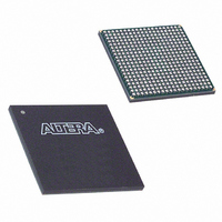
EP1C20F400C6N Altera, EP1C20F400C6N Datasheet - Page 42

EP1C20F400C6N
Manufacturer Part Number
EP1C20F400C6N
Description
IC CYCLONE FPGA 20K LE 400-FBGA
Manufacturer
Altera
Series
Cyclone®r
Datasheet
1.EP1C3T144C8.pdf
(106 pages)
Specifications of EP1C20F400C6N
Number Of Logic Elements/cells
20060
Number Of Labs/clbs
2006
Total Ram Bits
294912
Number Of I /o
301
Voltage - Supply
1.425 V ~ 1.575 V
Mounting Type
Surface Mount
Operating Temperature
0°C ~ 85°C
Package / Case
400-FBGA
Family Name
Cyclone®
Number Of Logic Blocks/elements
20060
# I/os (max)
301
Frequency (max)
405.2MHz
Process Technology
0.13um (CMOS)
Operating Supply Voltage (typ)
1.5V
Logic Cells
20060
Ram Bits
294912
Operating Supply Voltage (min)
1.425V
Operating Supply Voltage (max)
1.575V
Operating Temp Range
0C to 85C
Operating Temperature Classification
Commercial
Mounting
Surface Mount
Pin Count
400
Package Type
FBGA
Lead Free Status / RoHS Status
Lead free / RoHS Compliant
Number Of Gates
-
Lead Free Status / Rohs Status
Compliant
Other names
544-1687
Available stocks
Company
Part Number
Manufacturer
Quantity
Price
Company:
Part Number:
EP1C20F400C6N
Manufacturer:
ALTERA
Quantity:
237
Cyclone Device Handbook, Volume 1
2–36
Preliminary
External Clock Inputs
Each PLL supports single-ended or differential inputs for source-
synchronous receivers or for general-purpose use. The dedicated clock
pins (CLK[3..0]) feed the PLL inputs. These dual-purpose pins can also
act as LVDS input pins. See
Table 2–8
pins.
For more information on LVDS I/O support, refer to
page
External Clock Outputs
Each PLL supports one differential or one single-ended output for
source-synchronous transmitters or for general-purpose external clocks.
If the PLL does not use these PLL_OUT pins, the pins are available for use
as general-purpose I/O pins. The PLL_OUT pins support all I/O
standards shown in
The external clock outputs do not have their own V
supplies. Therefore, to minimize jitter, do not place switching I/O pins
next to these output pins. The EP1C3 device in the 100-pin TQFP package
3.3-V LVTTL/LVCMOS
2.5-V LVTTL/LVCMOS
1.8-V LVTTL/LVCMOS
1.5-V LVCMOS
3.3-V PCI
LVDS
SSTL-2 class I
SSTL-2 class II
SSTL-3 class I
SSTL-3 class II
Differential SSTL-2
Table 2–8. PLL I/O Standards
2–54.
I/O Standard
shows the I/O standards supported by PLL input and output
Table
2–8.
Figure
2–25.
CLK Input
v
v
v
v
v
v
v
v
v
v
—
CC
“LVDS I/O Pins” on
and ground voltage
Altera Corporation
EXTCLK Output
v
v
v
v
v
v
v
v
v
v
v
May 2008


