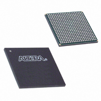
EP1C20F400C6N Altera, EP1C20F400C6N Datasheet - Page 39

EP1C20F400C6N
Manufacturer Part Number
EP1C20F400C6N
Description
IC CYCLONE FPGA 20K LE 400-FBGA
Manufacturer
Altera
Series
Cyclone®r
Datasheet
1.EP1C3T144C8.pdf
(106 pages)
Specifications of EP1C20F400C6N
Number Of Logic Elements/cells
20060
Number Of Labs/clbs
2006
Total Ram Bits
294912
Number Of I /o
301
Voltage - Supply
1.425 V ~ 1.575 V
Mounting Type
Surface Mount
Operating Temperature
0°C ~ 85°C
Package / Case
400-FBGA
Family Name
Cyclone®
Number Of Logic Blocks/elements
20060
# I/os (max)
301
Frequency (max)
405.2MHz
Process Technology
0.13um (CMOS)
Operating Supply Voltage (typ)
1.5V
Logic Cells
20060
Ram Bits
294912
Operating Supply Voltage (min)
1.425V
Operating Supply Voltage (max)
1.575V
Operating Temp Range
0C to 85C
Operating Temperature Classification
Commercial
Mounting
Surface Mount
Pin Count
400
Package Type
FBGA
Lead Free Status / RoHS Status
Lead free / RoHS Compliant
Number Of Gates
-
Lead Free Status / Rohs Status
Compliant
Other names
544-1687
Available stocks
Company
Part Number
Manufacturer
Quantity
Price
Company:
Part Number:
EP1C20F400C6N
Manufacturer:
ALTERA
Quantity:
237
Figure 2–25. Cyclone PLL
Notes to
(1)
(2)
(3)
Altera Corporation
May 2008
LVDSCLK1p (2)
LVDSCLK1n (2)
The EP1C3 device in the 100-pin TQFP package does not support external outputs or LVDS inputs. The EP1C6
device in the 144-pin TQFP package does not support external output from PLL2.
LVDS input is supported via the secondary function of the dedicated clock pins. For PLL 1, the CLK0 pin’s secondary
function is LVDSCLK1p and the CLK1 pin’s secondary function is LVDSCLK1n. For PLL 2, the CLK2 pin’s secondary
function is LVDSCLK2p and the CLK3 pin’s secondary function is LVDSCLK2n.
PFD: phase frequency detector.
CLK0 or
CLK1 or
Figure
2–25:
Table 2–6
a Cyclone PLL.
Notes to
(1)
(2)
(3)
(4)
Note (1)
Clock multiplication and division
Phase shift
Programmable duty cycle
Number of internal clock outputs
Number of external clock outputs
Table 2–6. Cyclone PLL Features
÷n
The m counter ranges from 2 to 32. The n counter and the post-scale counters
range from 1 to 32.
The smallest phase shift is determined by the voltage-controlled oscillator (VCO)
period divided by 8.
For degree increments, Cyclone devices can shift all output frequencies in
increments of 45°. Smaller degree increments are possible depending on the
frequency and divide parameters.
The EP1C3 device in the 100-pin TQFP package does not support external clock
output. The EP1C6 device in the 144-pin TQFP package does not support external
clock output from PLL2.
Δt
Table
shows the PLL features in Cyclone devices.
PFD (3)
2–6:
Feature
Δt
Charge
Pump
÷m
Global Clock Network and Phase-Locked Loops
Loop
Filter
m/(n × post-scale counter)
Down to 125-ps increments (2),
Yes
2
One differential or one single-ended
VCO
Selectable at Each PLL
VCO Phase Selection
Output Port
PLL Support
Figure 2–25
Post-Scale
Counters
÷g0
÷g1
÷e
(1)
Preliminary
Global clock
Global clock
I/O buffer
(3)
shows
2–33
(4)


