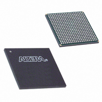
EP1C20F400C6N Altera, EP1C20F400C6N Datasheet - Page 34

EP1C20F400C6N
Manufacturer Part Number
EP1C20F400C6N
Description
IC CYCLONE FPGA 20K LE 400-FBGA
Manufacturer
Altera
Series
Cyclone®r
Datasheet
1.EP1C3T144C8.pdf
(106 pages)
Specifications of EP1C20F400C6N
Number Of Logic Elements/cells
20060
Number Of Labs/clbs
2006
Total Ram Bits
294912
Number Of I /o
301
Voltage - Supply
1.425 V ~ 1.575 V
Mounting Type
Surface Mount
Operating Temperature
0°C ~ 85°C
Package / Case
400-FBGA
Family Name
Cyclone®
Number Of Logic Blocks/elements
20060
# I/os (max)
301
Frequency (max)
405.2MHz
Process Technology
0.13um (CMOS)
Operating Supply Voltage (typ)
1.5V
Logic Cells
20060
Ram Bits
294912
Operating Supply Voltage (min)
1.425V
Operating Supply Voltage (max)
1.575V
Operating Temp Range
0C to 85C
Operating Temperature Classification
Commercial
Mounting
Surface Mount
Pin Count
400
Package Type
FBGA
Lead Free Status / RoHS Status
Lead free / RoHS Compliant
Number Of Gates
-
Lead Free Status / Rohs Status
Compliant
Other names
544-1687
Available stocks
Company
Part Number
Manufacturer
Quantity
Price
Company:
Part Number:
EP1C20F400C6N
Manufacturer:
ALTERA
Quantity:
237
Cyclone Device Handbook, Volume 1
Figure 2–20. Read/Write Clock Mode in Simple Dual-Port Mode
Notes to
(1)
(2)
2–28
Preliminary
wraddress[ ]
address[ ]
byteena[ ]
wrclken
wrclock
rdclken
rdclock
All registers shown except the rden register have asynchronous clear ports.
Violating the setup or hold time on the address registers could corrupt the memory contents. This applies to both
read and write operations.
data[ ]
wren
rden
Figure
6 LAB Row
Clocks
6
2–20:
Read/Write Clock Mode
The M4K memory blocks implement read/write clock mode for simple
dual-port memory. You can use up to two clocks in this mode. The write
clock controls the block's data inputs, wraddress, and wren. The read
clock controls the data output, rdaddress, and rden. The memory
blocks support independent clock enables for each clock and
asynchronous clear signals for the read- and write-side registers.
Figure 2–20
D
ENA
D
ENA
D
ENA
D
ENA
D
ENA
D
ENA
shows a memory block in read/write clock mode.
Q
Q
Q
Q
Q
Q
Generator
Pulse
Write
Data In
Read Address
Write Address
Byte Enable
Read Enable
Write Enable
Notes
Memory Block
1,024 × 4
2,048 × 2
4,096 × 1
Data Out
256 × 16
512 × 8
(1),
(2)
D
ENA
Q
Altera Corporation
To MultiTrack
Interconnect
May 2008


