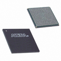
EP1C20F400C6N Altera, EP1C20F400C6N Datasheet - Page 4

EP1C20F400C6N
Manufacturer Part Number
EP1C20F400C6N
Description
IC CYCLONE FPGA 20K LE 400-FBGA
Manufacturer
Altera
Series
Cyclone®r
Datasheet
1.EP1C3T144C8.pdf
(106 pages)
Specifications of EP1C20F400C6N
Number Of Logic Elements/cells
20060
Number Of Labs/clbs
2006
Total Ram Bits
294912
Number Of I /o
301
Voltage - Supply
1.425 V ~ 1.575 V
Mounting Type
Surface Mount
Operating Temperature
0°C ~ 85°C
Package / Case
400-FBGA
Family Name
Cyclone®
Number Of Logic Blocks/elements
20060
# I/os (max)
301
Frequency (max)
405.2MHz
Process Technology
0.13um (CMOS)
Operating Supply Voltage (typ)
1.5V
Logic Cells
20060
Ram Bits
294912
Operating Supply Voltage (min)
1.425V
Operating Supply Voltage (max)
1.575V
Operating Temp Range
0C to 85C
Operating Temperature Classification
Commercial
Mounting
Surface Mount
Pin Count
400
Package Type
FBGA
Lead Free Status / RoHS Status
Lead free / RoHS Compliant
Number Of Gates
-
Lead Free Status / Rohs Status
Compliant
Other names
544-1687
Available stocks
Company
Part Number
Manufacturer
Quantity
Price
Company:
Part Number:
EP1C20F400C6N
Manufacturer:
ALTERA
Quantity:
237
Cyclone Device Handbook, Volume 1
1–2
Preliminary
Note to
(1)
Notes to
(1)
(2)
Total RAM bits
PLLs
Maximum user I/O pins
EP1C3
EP1C4
EP1C6
EP1C12
EP1C20
Table 1–1. Cyclone Device Features (Part 2 of 2)
Table 1–2. Cyclone Package Options and I/O Pin Counts
Device
This parameter includes global clock pins.
TQFP: thin quad flat pack.
PQFP: plastic quad flat pack.
Cyclone devices support vertical migration within the same package (i.e., designers can migrate between the
EP1C3 device in the 144-pin TQFP package and the EP1C6 device in the same package).
Table
Table
Feature
1–1:
100-Pin TQFP
1–2:
(1)
65
—
—
—
—
(1)
Cyclone devices are available in quad flat pack (QFP) and space-saving
FineLine
Vertical migration means you can migrate a design from one device to
another that has the same dedicated pins, JTAG pins, and power pins, and
are subsets or supersets for a given package across device densities. The
largest density in any package has the highest number of power pins; you
must use the layout for the largest planned density in a package to
provide the necessary power pins for migration.
For I/O pin migration across densities, cross-reference the available I/O
pins using the device pin-outs for all planned densities of a given package
type to identify which I/O pins can be migrated. The Quartus
software can automatically cross-reference and place all pins for you
when given a device migration list. If one device has power or ground
pins, but these same pins are user I/O on a different device that is in the
migration path,the Quartus II software ensures the pins are not used as
user I/O in the Quartus II software. Ensure that these pins are connected
144-Pin TQFP
(1),
104
98
—
—
—
(2)
59,904
EP1C3
®
104
BGA packages (see
1
240-Pin PQFP
185
173
(1)
—
—
—
78,336
EP1C4
301
2
FineLine BGA
Tables 1–2
256-Pin
185
185
—
—
—
92,160
EP1C6
185
2
through 1–3).
FineLine BGA
324-Pin
239,616
EP1C12
249
249
233
—
—
249
2
Altera Corporation
FineLine BGA
400-Pin
®
294,912
EP1C20
May 2008
301
301
II
301
—
—
—
2


