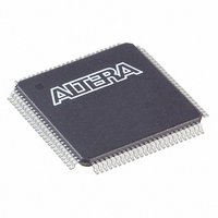
EP1C3T100C7 Altera, EP1C3T100C7 Datasheet - Page 49

EP1C3T100C7
Manufacturer Part Number
EP1C3T100C7
Description
IC CYCLONE FPGA 2910 LE 100-TQFP
Manufacturer
Altera
Series
Cyclone®r
Datasheet
1.EP1C3T144C8.pdf
(106 pages)
Specifications of EP1C3T100C7
Number Of Logic Elements/cells
2910
Number Of Labs/clbs
291
Total Ram Bits
59904
Number Of I /o
65
Voltage - Supply
1.425 V ~ 1.575 V
Mounting Type
Surface Mount
Operating Temperature
0°C ~ 85°C
Package / Case
100-TQFP, 100-VQFP
Lead Free Status / RoHS Status
Contains lead / RoHS non-compliant
Number Of Gates
-
Other names
544-1015
Available stocks
Company
Part Number
Manufacturer
Quantity
Price
Company:
Part Number:
EP1C3T100C7
Manufacturer:
ALTERA
Quantity:
455
Part Number:
EP1C3T100C7
Manufacturer:
ALTERA
Quantity:
20 000
Company:
Part Number:
EP1C3T100C7N
Manufacturer:
ALTERA
Quantity:
364
Part Number:
EP1C3T100C7N
Manufacturer:
ALTERA
Quantity:
20 000
Figure 2–30. Signal Path through the I/O Block
Altera Corporation
May 2008
From Logic
To Logic
Array
Array
comb_io_datain
Row or Column
io_clk[5..0]
io_cce_out
io_dataout
io_cce_in
io_datain
io_caclr
io_csclr
io_cclk
io_coe
The pin's datain signals can drive the logic array. The logic array drives
the control and data signals, providing a flexible routing resource. The
row or column IOE clocks, io_clk[5..0], provide a dedicated routing
resource for low-skew, high-speed clocks. The global clock network
generates the IOE clocks that feed the row or column I/O regions (see
“Global Clock Network and Phase-Locked Loops” on page
Figure 2–30
Each IOE contains its own control signal selection for the following
control signals: oe, ce_in, ce_out, aclr/preset, sclr/preset,
clk_in, and clk_out.
selection.
Data and
Selection
Control
Signal
illustrates the signal paths through the I/O block.
oe
ce_in
ce_out
aclr/preset
sclr
clk_in
clk_out
dataout
Figure 2–31
To Other
IOEs
illustrates the control signal
IOE
2–29).
I/O Structure
Preliminary
2–43


