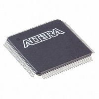
EP1C3T100C7 Altera, EP1C3T100C7 Datasheet - Page 35

EP1C3T100C7
Manufacturer Part Number
EP1C3T100C7
Description
IC CYCLONE FPGA 2910 LE 100-TQFP
Manufacturer
Altera
Series
Cyclone®r
Datasheet
1.EP1C3T144C8.pdf
(106 pages)
Specifications of EP1C3T100C7
Number Of Logic Elements/cells
2910
Number Of Labs/clbs
291
Total Ram Bits
59904
Number Of I /o
65
Voltage - Supply
1.425 V ~ 1.575 V
Mounting Type
Surface Mount
Operating Temperature
0°C ~ 85°C
Package / Case
100-TQFP, 100-VQFP
Lead Free Status / RoHS Status
Contains lead / RoHS non-compliant
Number Of Gates
-
Other names
544-1015
Available stocks
Company
Part Number
Manufacturer
Quantity
Price
Company:
Part Number:
EP1C3T100C7
Manufacturer:
ALTERA
Quantity:
455
Part Number:
EP1C3T100C7
Manufacturer:
ALTERA
Quantity:
20 000
Company:
Part Number:
EP1C3T100C7N
Manufacturer:
ALTERA
Quantity:
364
Part Number:
EP1C3T100C7N
Manufacturer:
ALTERA
Quantity:
20 000
Figure 2–21. Single-Port Mode
Note to
(1)
Global Clock
Network and
Phase-Locked
Loops
Altera Corporation
May 2008
address[ ]
outclken
outclock
inclken
inclock
data[ ]
wren
Violating the setup or hold time on the address registers could corrupt the memory contents. This applies to both
read and write operations.
Figure
6 LAB Row
Clocks
6
2–21:
Single-Port Mode
The M4K memory blocks also support single-port mode, used when
simultaneous reads and writes are not required. See
M4K memory block can support up to two single-port mode RAM blocks
if each RAM block is less than or equal to 2K bits in size.
Cyclone devices provide a global clock network and up to two PLLs for a
complete clock management solution.
Global Clock Network
There are four dedicated clock pins (CLK[3..0], two pins on the left side
and two pins on the right side) that drive the global clock network, as
shown in
(DPCLK[7..0]) pins can also drive the global clock network.
Note (1)
D
ENA
D
ENA
Figure
Q
Q
2–22. PLL outputs, logic array, and dual-purpose clock
Generator
D
ENA
Pulse
Write
Q
Global Clock Network and Phase-Locked Loops
Data In
Address
Write Enable
RAM/ROM
1,024 × 4
2,048 × 2
4,096 × 1
Data Out
256 × 16
512 × 8
D
ENA
Figure
Q
2–21. A single
Preliminary
To MultiTrack
Interconnect
2–29


