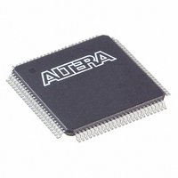
EP1C3T100C7 Altera, EP1C3T100C7 Datasheet - Page 32

EP1C3T100C7
Manufacturer Part Number
EP1C3T100C7
Description
IC CYCLONE FPGA 2910 LE 100-TQFP
Manufacturer
Altera
Series
Cyclone®r
Datasheet
1.EP1C3T144C8.pdf
(106 pages)
Specifications of EP1C3T100C7
Number Of Logic Elements/cells
2910
Number Of Labs/clbs
291
Total Ram Bits
59904
Number Of I /o
65
Voltage - Supply
1.425 V ~ 1.575 V
Mounting Type
Surface Mount
Operating Temperature
0°C ~ 85°C
Package / Case
100-TQFP, 100-VQFP
Lead Free Status / RoHS Status
Contains lead / RoHS non-compliant
Number Of Gates
-
Other names
544-1015
Available stocks
Company
Part Number
Manufacturer
Quantity
Price
Company:
Part Number:
EP1C3T100C7
Manufacturer:
ALTERA
Quantity:
455
Part Number:
EP1C3T100C7
Manufacturer:
ALTERA
Quantity:
20 000
Company:
Part Number:
EP1C3T100C7N
Manufacturer:
ALTERA
Quantity:
364
Part Number:
EP1C3T100C7N
Manufacturer:
ALTERA
Quantity:
20 000
Cyclone Device Handbook, Volume 1
Figure 2–18. Input/Output Clock Mode in True Dual-Port Mode
Notes to
(1)
(2)
2–26
Preliminary
clken
clock
wren
A
A
A
data
byteena
address
All registers shown have asynchronous clear ports.
Violating the setup or hold time on the address registers could corrupt the memory contents. This applies to both
read and write operations.
A
[ ]
6
A
A
[ ]
Figure
[ ]
6 LAB Row Clocks
2–18:
D
ENA
D
ENA
D
ENA
D
ENA
Q
Q
Q
Q
Generator
Pulse
Write
D
ENA
Data In
Byte Enable A
Address A
Write/Read
Enable
Data Out
Q
A
Memory Block
256 × 16 (2)
q
1,024 × 4
2,048 × 2
4,096 × 1
A
512 × 8
[ ]
q
B
[ ]
Byte Enable B
Write/Read
Address B
Data Out
B
Data In
Enable
Q
ENA
D
Notes
Generator
Write
Pulse
(1),
(2)
Q
Q
Q
Q
ENA
ENA
ENA
ENA
D
D
D
D
Altera Corporation
May 2008
6
data
byteena
address
wren
clken
clock
B
B
B
B
[ ]
B
B
[ ]
[ ]


