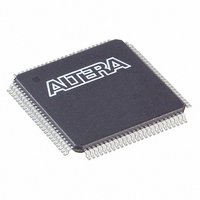
EP1C3T100C7 Altera, EP1C3T100C7 Datasheet - Page 57

EP1C3T100C7
Manufacturer Part Number
EP1C3T100C7
Description
IC CYCLONE FPGA 2910 LE 100-TQFP
Manufacturer
Altera
Series
Cyclone®r
Datasheet
1.EP1C3T144C8.pdf
(106 pages)
Specifications of EP1C3T100C7
Number Of Logic Elements/cells
2910
Number Of Labs/clbs
291
Total Ram Bits
59904
Number Of I /o
65
Voltage - Supply
1.425 V ~ 1.575 V
Mounting Type
Surface Mount
Operating Temperature
0°C ~ 85°C
Package / Case
100-TQFP, 100-VQFP
Lead Free Status / RoHS Status
Contains lead / RoHS non-compliant
Number Of Gates
-
Other names
544-1015
Available stocks
Company
Part Number
Manufacturer
Quantity
Price
Company:
Part Number:
EP1C3T100C7
Manufacturer:
ALTERA
Quantity:
455
Part Number:
EP1C3T100C7
Manufacturer:
ALTERA
Quantity:
20 000
Company:
Part Number:
EP1C3T100C7N
Manufacturer:
ALTERA
Quantity:
364
Part Number:
EP1C3T100C7N
Manufacturer:
ALTERA
Quantity:
20 000
Altera Corporation
May 2008
Slew-Rate Control
The output buffer for each Cyclone device I/O pin has a programmable
output slew-rate control that can be configured for low noise or
high-speed performance. A faster slew rate provides high-speed
transitions for high-performance systems. However, these fast transitions
may introduce noise transients into the system. A slow slew rate reduces
system noise, but adds a nominal delay to rising and falling edges. Each
I/O pin has an individual slew-rate control, allowing the designer to
specify the slew rate on a pin-by-pin basis. The slew-rate control affects
both the rising and falling edges.
Bus Hold
Each Cyclone device I/O pin provides an optional bus-hold feature. The
bus-hold circuitry can hold the signal on an I/O pin at its last-driven
state. Since the bus-hold feature holds the last-driven state of the pin until
the next input signal is present, an external pull-up or pull-down resistor
is not necessary to hold a signal level when the bus is tri-stated.
The bus-hold circuitry also pulls undriven pins away from the input
threshold voltage where noise can cause unintended high-frequency
switching. The designer can select this feature individually for each I/O
pin. The bus-hold output will drive no higher than V
overdriving signals. If the bus-hold feature is enabled, the device cannot
use the programmable pull-up option. Disable the bus-hold feature when
the I/O pin is configured for differential signals.
The bus-hold circuitry uses a resistor with a nominal resistance (RBH) of
approximately 7 kΩ to pull the signal level to the last-driven state.
Table 4–15 on page 4–6
V
used to identify the next-driven input level.
The bus-hold circuitry is only active after configuration. When going into
user mode, the bus-hold circuit captures the value on the pin present at
the end of configuration.
Programmable Pull-Up Resistor
Each Cyclone device I/O pin provides an optional programmable
pull-up resistor during user mode. If the designer enables this feature for
an I/O pin, the pull-up resistor (typically 25 kΩ) holds the output to the
V
optional programmable pull-up resistor.
CCIO
CCIO
level of the output pin's bank. Dedicated clock pins do not have the
voltage level driven through this resistor and overdrive current
gives the specific sustaining current for each
CCIO
to prevent
I/O Structure
Preliminary
2–51


