EP1C3T100C7 Altera, EP1C3T100C7 Datasheet - Page 26
EP1C3T100C7
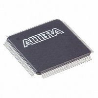
Manufacturer Part Number
EP1C3T100C7
Description
IC CYCLONE FPGA 2910 LE 100-TQFP
Manufacturer
Altera
Series
Cyclone®r
Datasheet
1.EP1C3T144C8.pdf
(106 pages)
Specifications of EP1C3T100C7
Number Of Logic Elements/cells
2910
Number Of Labs/clbs
291
Total Ram Bits
59904
Number Of I /o
65
Voltage - Supply
1.425 V ~ 1.575 V
Mounting Type
Surface Mount
Operating Temperature
0°C ~ 85°C
Package / Case
100-TQFP, 100-VQFP
Lead Free Status / RoHS Status
Contains lead / RoHS non-compliant
Number Of Gates
-
Other names
544-1015
Available stocks
Company
Part Number
Manufacturer
Quantity
Price
Company:

Part Number:
EP1C3T100C7
Manufacturer:
ALTERA
Quantity:
455
Part Number:
EP1C3T100C7
Manufacturer:
ALTERA
Quantity:
20 000
Company:
Part Number:
EP1C3T100C7N
Manufacturer:
ALTERA
Quantity:
364
Part Number:
EP1C3T100C7N
Manufacturer:
ALTERA
Quantity:
20 000


Cyclone Device Handbook, Volume 1
2–20
Preliminary
signal. The output registers can be bypassed. Pseudo-asynchronous
reading is possible in the simple dual-port mode of M4K blocks by
clocking the read enable and read address registers on the negative clock
edge and bypassing the output registers.
When configured as RAM or ROM, you can use an initialization file to
pre-load the memory contents.
Two single-port memory blocks can be implemented in a single M4K
block as long as each of the two independent block sizes is equal to or less
than half of the M4K block size.
The Quartus II software automatically implements larger memory by
combining multiple M4K memory blocks. For example, two 256×16-bit
RAM blocks can be combined to form a 256×32-bit RAM block. Memory
performance does not degrade for memory blocks using the maximum
number of words allowed. Logical memory blocks using less than the
maximum number of words use physical blocks in parallel, eliminating
any external control logic that would increase delays. To create a larger
high-speed memory block, the Quartus II software automatically
combines memory blocks with LE control logic.
Parity Bit Support
The M4K blocks support a parity bit for each byte. The parity bit, along
with internal LE logic, can implement parity checking for error detection
to ensure data integrity. You can also use parity-size data words to store
user-specified control bits. Byte enables are also available for data input
masking during write operations.
Shift Register Support
You can configure M4K memory blocks to implement shift registers for
DSP applications such as pseudo-random number generators,
multi-channel filtering, auto-correlation, and cross-correlation functions.
These and other DSP applications require local data storage, traditionally
implemented with standard flip-flops, which can quickly consume many
logic cells and routing resources for large shift registers. A more efficient
alternative is to use embedded memory as a shift register block, which
saves logic cell and routing resources and provides a more efficient
implementation with the dedicated circuitry.
The size of a w × m × n shift register is determined by the input data width
(w), the length of the taps (m), and the number of taps (n). The size of a
w × m × n shift register must be less than or equal to the maximum number
of memory bits in the M4K block (4,608 bits). The total number of shift
Altera Corporation
May 2008
Related parts for EP1C3T100C7
Image
Part Number
Description
Manufacturer
Datasheet
Request
R

Part Number:
Description:
CYCLONE II STARTER KIT EP2C20N
Manufacturer:
Altera
Datasheet:


Part Number:
Description:
CPLD, EP610 Family, ECMOS Process, 300 Gates, 16 Macro Cells, 16 Reg., 16 User I/Os, 5V Supply, 35 Speed Grade, 24DIP
Manufacturer:
Altera Corporation
Datasheet:
Part Number:
Description:
CPLD, EP610 Family, ECMOS Process, 300 Gates, 16 Macro Cells, 16 Reg., 16 User I/Os, 5V Supply, 15 Speed Grade, 24DIP
Manufacturer:
Altera Corporation
Datasheet:
Part Number:
Description:
Manufacturer:
Altera Corporation
Datasheet:
Part Number:
Description:
CPLD, EP610 Family, ECMOS Process, 300 Gates, 16 Macro Cells, 16 Reg., 16 User I/Os, 5V Supply, 30 Speed Grade, 24DIP
Manufacturer:
Altera Corporation
Datasheet:
Part Number:
Description:
High-performance, low-power erasable programmable logic devices with 8 macrocells, 10ns
Manufacturer:
Altera Corporation
Datasheet:
Part Number:
Description:
High-performance, low-power erasable programmable logic devices with 8 macrocells, 7ns
Manufacturer:
Altera Corporation
Datasheet:
Part Number:
Description:
Classic EPLD
Manufacturer:
Altera Corporation
Datasheet:
Part Number:
Description:
High-performance, low-power erasable programmable logic devices with 8 macrocells, 10ns
Manufacturer:
Altera Corporation
Datasheet:
Part Number:
Description:
Manufacturer:
Altera Corporation
Datasheet:
Part Number:
Description:
Manufacturer:
Altera Corporation
Datasheet:
Part Number:
Description:
Manufacturer:
Altera Corporation
Datasheet:
Part Number:
Description:
CPLD, EP610 Family, ECMOS Process, 300 Gates, 16 Macro Cells, 16 Reg., 16 User I/Os, 5V Supply, 25 Speed Grade, 24DIP
Manufacturer:
Altera Corporation
Datasheet: