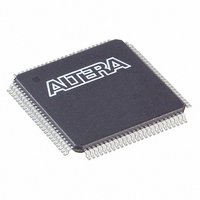
EP1C3T100C7 Altera, EP1C3T100C7 Datasheet - Page 42

EP1C3T100C7
Manufacturer Part Number
EP1C3T100C7
Description
IC CYCLONE FPGA 2910 LE 100-TQFP
Manufacturer
Altera
Series
Cyclone®r
Datasheet
1.EP1C3T144C8.pdf
(106 pages)
Specifications of EP1C3T100C7
Number Of Logic Elements/cells
2910
Number Of Labs/clbs
291
Total Ram Bits
59904
Number Of I /o
65
Voltage - Supply
1.425 V ~ 1.575 V
Mounting Type
Surface Mount
Operating Temperature
0°C ~ 85°C
Package / Case
100-TQFP, 100-VQFP
Lead Free Status / RoHS Status
Contains lead / RoHS non-compliant
Number Of Gates
-
Other names
544-1015
Available stocks
Company
Part Number
Manufacturer
Quantity
Price
Company:
Part Number:
EP1C3T100C7
Manufacturer:
ALTERA
Quantity:
455
Part Number:
EP1C3T100C7
Manufacturer:
ALTERA
Quantity:
20 000
Company:
Part Number:
EP1C3T100C7N
Manufacturer:
ALTERA
Quantity:
364
Part Number:
EP1C3T100C7N
Manufacturer:
ALTERA
Quantity:
20 000
Cyclone Device Handbook, Volume 1
2–36
Preliminary
External Clock Inputs
Each PLL supports single-ended or differential inputs for source-
synchronous receivers or for general-purpose use. The dedicated clock
pins (CLK[3..0]) feed the PLL inputs. These dual-purpose pins can also
act as LVDS input pins. See
Table 2–8
pins.
For more information on LVDS I/O support, refer to
page
External Clock Outputs
Each PLL supports one differential or one single-ended output for
source-synchronous transmitters or for general-purpose external clocks.
If the PLL does not use these PLL_OUT pins, the pins are available for use
as general-purpose I/O pins. The PLL_OUT pins support all I/O
standards shown in
The external clock outputs do not have their own V
supplies. Therefore, to minimize jitter, do not place switching I/O pins
next to these output pins. The EP1C3 device in the 100-pin TQFP package
3.3-V LVTTL/LVCMOS
2.5-V LVTTL/LVCMOS
1.8-V LVTTL/LVCMOS
1.5-V LVCMOS
3.3-V PCI
LVDS
SSTL-2 class I
SSTL-2 class II
SSTL-3 class I
SSTL-3 class II
Differential SSTL-2
Table 2–8. PLL I/O Standards
2–54.
I/O Standard
shows the I/O standards supported by PLL input and output
Table
2–8.
Figure
2–25.
CLK Input
v
v
v
v
v
v
v
v
v
v
—
CC
“LVDS I/O Pins” on
and ground voltage
Altera Corporation
EXTCLK Output
v
v
v
v
v
v
v
v
v
v
v
May 2008


