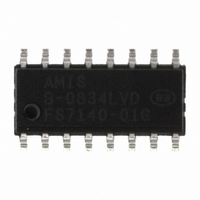
FS7140-01G-XTD ON Semiconductor, FS7140-01G-XTD Datasheet - Page 8

FS7140-01G-XTD
Manufacturer Part Number
FS7140-01G-XTD
Description
IC CLOCK GEN PLL PROGR 16-SOIC
Manufacturer
ON Semiconductor
Type
PLL Clock Generatorr
Datasheet
1.FS7145-01-XTP.pdf
(19 pages)
Specifications of FS7140-01G-XTD
Pll
Yes
Input
Crystal
Output
CMOS, PECL
Number Of Circuits
1
Ratio - Input:output
2:1
Differential - Input:output
No/Yes
Frequency - Max
400MHz
Divider/multiplier
Yes/No
Voltage - Supply
3 V ~ 3.6 V
Operating Temperature
0°C ~ 70°C
Mounting Type
Surface Mount
Package / Case
16-SOIC (3.9mm Width)
Frequency-max
340MHz
Mounting Style
SMD/SMT
Max Input Freq
80 MHz
Max Output Freq
340 MHz
Number Of Outputs
1
Operating Supply Voltage
3.3 V
Operating Temperature Range
0 C to + 70 C
Supply Current
35 mA
Lead Free Status / RoHS Status
Lead free / RoHS Compliant
Other names
766-1028
Available stocks
Company
Part Number
Manufacturer
Quantity
Price
Company:
Part Number:
FS7140-01G-XTD
Manufacturer:
ON
Quantity:
1 789
FS714x
5.2.3. Random Register Read Procedure
Random read operations allow the master to directly read from any register. To perform a read procedure, the R/W bit that is
transmitted after the seven-bit address is a logic-low, as in the register write procedure. This indicates to the addressed slave device
that a register address will follow after the slave device acknowledges its device address. The register address is then written into the
slave's address pointer.
Following an acknowledge by the slave, the master generates a repeated START condition. The repeated START terminates the write
procedure, but not until after the slave's address pointer is set. The slave address is then resent, with the R/W bit set this time to a
logic-high, indicating to the slave that data will be read. The slave will acknowledge the device address, and then transmits the eight-bit
word. The master does not acknowledge the transfer but does generate a STOP condition.
5.2.4. Sequential Register Write Procedure
Sequential write operations allow the master to write to each register in order. The register pointer is automatically incremented after
each write. This procedure is more efficient than the random register write if several registers must be written.
To initiate a write procedure, the R/W bit that is transmitted after the seven-bit device address is a logic-low. This indicates to the
addressed slave device that a register address will follow after the slave device acknowledges its device address. The register address
is written into the slave's address pointer. Following an acknowledge by the slave, the master is allowed to write up to eight bytes of
data into the addressed register before the register address pointer overflows back to the beginning address.
An acknowledge by the device between each byte of data must occur before the next data byte is sent.
Registers are updated every time the device sends an acknowledge to the host. The register update does not wait for the STOP
condition to occur. Registers are therefore updated at different times during a sequential register write.
5.2.5. Sequential Register Read Procedure
Sequential read operations allow the master to read from each register in order. The register pointer is automatically incremented by
one after each read. This procedure is more efficient than the random register read if several registers must be read.
To perform a read procedure, the R/W bit that is transmitted after the seven-bit address is a logic-low, as in the register write procedure.
This indicates to the addressed slave device that a register address will follow after the slave device acknowledges its device address.
The register address is then written into the slave's address pointer.
Following an acknowledge by the slave, the master generates a repeated START condition. The repeated START terminates the write
procedure, but not until after the slave's address pointer is set. The slave address is then resent, with the R/W bit set this time to a
logic-high, indicating to the slave that data will be read. The slave will acknowledge the device address, and then transmits all eight
bytes of data starting with the initial addressed register. The register address pointer will overflow if the initial register address is larger
than zero. After the last byte of data, the master does not acknowledge the transfer but does generate a STOP condition.
Rev. 5 | Page 8 of 19 | www.onsemi.com


