FS7140-01G-XTD ON Semiconductor, FS7140-01G-XTD Datasheet - Page 11
FS7140-01G-XTD
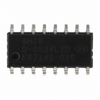
Manufacturer Part Number
FS7140-01G-XTD
Description
IC CLOCK GEN PLL PROGR 16-SOIC
Manufacturer
ON Semiconductor
Type
PLL Clock Generatorr
Datasheet
1.FS7145-01-XTP.pdf
(19 pages)
Specifications of FS7140-01G-XTD
Pll
Yes
Input
Crystal
Output
CMOS, PECL
Number Of Circuits
1
Ratio - Input:output
2:1
Differential - Input:output
No/Yes
Frequency - Max
400MHz
Divider/multiplier
Yes/No
Voltage - Supply
3 V ~ 3.6 V
Operating Temperature
0°C ~ 70°C
Mounting Type
Surface Mount
Package / Case
16-SOIC (3.9mm Width)
Frequency-max
340MHz
Mounting Style
SMD/SMT
Max Input Freq
80 MHz
Max Output Freq
340 MHz
Number Of Outputs
1
Operating Supply Voltage
3.3 V
Operating Temperature Range
0 C to + 70 C
Supply Current
35 mA
Lead Free Status / RoHS Status
Lead free / RoHS Compliant
Other names
766-1028
Available stocks
Company
Part Number
Manufacturer
Quantity
Price
Company:

Part Number:
FS7140-01G-XTD
Manufacturer:
ON
Quantity:
1 789


FS714x
6.0 Programming Information
All register bits are cleared to zero on power-up. All register bits may be read back as written.
Table 3: FS7140 Register Map
Address
Byte 7
Byte 6
Byte 5
Byte 4
Byte 3
Byte 2
Byte 1
Byte 0
Must be set to “0”
Must be set to “0”
Must be set to “0”
FBKDIV[7]
REFDIV[7]
Reserved
Reserved
Reserved
POST2[3]
POST3[1]
Modulus = 1,2,4, or 8; See Table 8
1 = CMOS
0 = PECL
CMOS
BIT 7
(Bit 63)
(Bit 55)
(Bit 47)
(Bit 39)
(Bit 31)
(Bit 23)
(Bit 15)
(Bit 7)
128
128
Modulus = N +1 (N = 0 to 11); See Table 8
Must be set to “0”
Must be set to “0”
0 = VCO output
1 = Post divider
FBKDSRC
REFDIV[6]
Loop filter cap
FBKDIV[6]
POST2[2]
POST3[0]
Reserved
Reserved
BIT 6
(Bit 62)
(Bit 54)
(Bit 46)
(Bit 38)
(Bit 30)
(Bit 22)
(Bit 14)
output
select
(Bit 6)
LC
64
64
1 = Powered down
1 = Powered down
Must be set to “0”
FBKDIV[13]
FBKDIV[5]
REFDIV[5]
Reserved
POST2[1]
0 = Normal
0 = Normal
SHUT2
SHUT1
BIT 5
(Bit 61)
(Bit 53)
LR[1]
(Bit 45)
(Bit 29)
(Bit 21)
(Bit 13)
(Bit 37)
(Bit 5)
8192
32
32
Loop filter resistor select
Rev. 5 | Page 11 of 19 | www.onsemi.com
See Section 4.1.2 for disallowed FBKDIV values
Must be set to “0”
Must be set to “0”
FBKDIV[12]
FBKDIV[4]
REFDSRC
REFDIV[4]
Reserved
Reserved
POST2[0]
1 = REF pin
0 = Crystal
oscillator
BIT 4
(Bit 60)
(Bit 52)
LR[0]
(Bit 44)
(Bit 36)
(Bit 20)
(Bit 12)
(Bit 28)
(Bit 4)
4096
16
16
See Section 4.1.2 for disallowed FBKDIV values
Must be set to “0”
Must be set to “0”
Must be set to “0”
FBKDIV[11]
REFDIV[11]
REFDIV[3]
FBKDIV[3]
POST1[3]
Reserved
Reserved
Reserved
BIT 3
(Bit 59)
(Bit 51)
(Bit 43)
(Bit 35)
(Bit 27)
(Bit 19)
(Bit 11)
(Bit 3)
2048
2048
8
8
Must be set to “0”
Must be set to “0”
Must be set to “0”
FBKDIV[10]
REFDIV[10]
FBKDIV[2]
REFDIV[2]
POST1[2]
Reserved
Reserved
Reserved
BIT 2
(Bit 58)
(Bit 50)
(Bit 42)
(Bit 34)
(Bit 26)
(Bit 18)
(Bit 10)
(Bit 2)
1024
1024
4
4
Modulus = N +1 (N = 0 to 11); See Table 8
Must be set to “0”
Must be set to “0”
REFDIV[9]
REFDIV[1]
FBKDIV[9]
FBKDIV[1]
POST1[1]
Reserved
Reserved
BIT 1
(Bit 57)
(Bit 49)
CP[1]
(Bit 41)
(Bit 33)
(Bit 25)
(Bit 17)
(Bit 9)
(Bit 1)
Charge pump current select
512
512
2
2
Must be set to “0”
Must be set to “0”
FBKDIV[8]
FBKDIV[0]
REFDIV[8]
REFDIV[0]
POST1[0]
Reserved
Reserved
BIT 0
(Bit 56)
(Bit 48)
CP[0]
(Bit 40)
(Bit 32)
(Bit 24)
(Bit 16)
(Bit 8)
(Bit 0)
256
256
1
1
Related parts for FS7140-01G-XTD
Image
Part Number
Description
Manufacturer
Datasheet
Request
R

Part Number:
Description:
IC CLOCK GEN PLL PROGR 16-SSOP
Manufacturer:
ON Semiconductor
Datasheet:

Part Number:
Description:
IC CLOCK GEN PLL PROG 16SOIC
Manufacturer:
ON Semiconductor
Datasheet:
Part Number:
Description:
IC CLOCK GEN PLL PROG 16SSOP
Manufacturer:
ON Semiconductor
Datasheet:
Part Number:
Description:
Programmable Phase- Locked Loop Clock Generator
Manufacturer:
ON Semiconductor
Datasheet:

Part Number:
Description:
Programmable Phase-Locked Loop Clock Generator
Manufacturer:
AMI [AMI SEMICONDUCTOR]
Datasheet:
Part Number:
Description:
ON Semiconductor [VOLTAGE REGULATOR]
Manufacturer:
ON Semiconductor
Datasheet:
Part Number:
Description:
357-036-542-201 CARDEDGE 36POS DL .156 BLK LOPRO
Manufacturer:
ON Semiconductor
Datasheet:
Part Number:
Description:
357-036-542-201 CARDEDGE 36POS DL .156 BLK LOPRO
Manufacturer:
ON Semiconductor
Datasheet:
Part Number:
Description:
357-036-542-201 CARDEDGE 36POS DL .156 BLK LOPRO
Manufacturer:
ON Semiconductor
Datasheet:
Part Number:
Description:
357-036-542-201 CARDEDGE 36POS DL .156 BLK LOPRO
Manufacturer:
ON Semiconductor
Datasheet:
Part Number:
Description:
357-036-542-201 CARDEDGE 36POS DL .156 BLK LOPRO
Manufacturer:
ON Semiconductor
Datasheet:
Part Number:
Description:
357-036-542-201 CARDEDGE 36POS DL .156 BLK LOPRO
Manufacturer:
ON Semiconductor
Datasheet:
Part Number:
Description:
357-036-542-201 CARDEDGE 36POS DL .156 BLK LOPRO
Manufacturer:
ON Semiconductor
Datasheet:
Part Number:
Description:
357-036-542-201 CARDEDGE 36POS DL .156 BLK LOPRO
Manufacturer:
ON Semiconductor
Datasheet:
Part Number:
Description:
357-036-542-201 CARDEDGE 36POS DL .156 BLK LOPRO
Manufacturer:
ON Semiconductor
Datasheet: