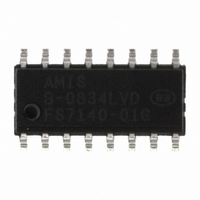
FS7140-01G-XTD ON Semiconductor, FS7140-01G-XTD Datasheet - Page 3

FS7140-01G-XTD
Manufacturer Part Number
FS7140-01G-XTD
Description
IC CLOCK GEN PLL PROGR 16-SOIC
Manufacturer
ON Semiconductor
Type
PLL Clock Generatorr
Datasheet
1.FS7145-01-XTP.pdf
(19 pages)
Specifications of FS7140-01G-XTD
Pll
Yes
Input
Crystal
Output
CMOS, PECL
Number Of Circuits
1
Ratio - Input:output
2:1
Differential - Input:output
No/Yes
Frequency - Max
400MHz
Divider/multiplier
Yes/No
Voltage - Supply
3 V ~ 3.6 V
Operating Temperature
0°C ~ 70°C
Mounting Type
Surface Mount
Package / Case
16-SOIC (3.9mm Width)
Frequency-max
340MHz
Mounting Style
SMD/SMT
Max Input Freq
80 MHz
Max Output Freq
340 MHz
Number Of Outputs
1
Operating Supply Voltage
3.3 V
Operating Temperature Range
0 C to + 70 C
Supply Current
35 mA
Lead Free Status / RoHS Status
Lead free / RoHS Compliant
Other names
766-1028
Available stocks
Company
Part Number
Manufacturer
Quantity
Price
Company:
Part Number:
FS7140-01G-XTD
Manufacturer:
ON
Quantity:
1 789
FS714x
Table 2: FS7145 Pin Descriptions
Pin
1
2
3
4
5
6
7
8
9
10
11
12
13
14
15
16
Key: AI: Analog Input; AO = Analog Output; DI = Digital Input; DI
DI-3 = Three-Level Digital Input; DO = Digital Output; P = Power/Ground; # = Active Low Pin
4.0 Functional Block Diagram
4.1 Phase Locked Loop (PLL)
The PLL is a standard phase- and frequency-locked loop architecture. The PLL consists of a reference divider, a phase-frequency
detector (PFD), a charge pump, an internal loop filter, a voltage-controlled oscillator (VCO), a feedback divider, and a post divider.
The reference frequency (generated by either the on-board crystal oscillator or an external frequency source), is first reduced by the
reference divider. The integer value that the frequency is divided by is called the modulus and is denoted as NR for the reference
divider. This divided reference is then fed into the PFD.
The VCO frequency is fed back to the PFD through the feedback divider (the modulus is denoted by NF).
The PFD will drive the VCO up or down in frequency until the divided reference frequency and the divided VCO frequency appearing at
the inputs of the PFD are equal. The input/output relationship between the reference frequency and the VCO frequency is then:
This basic PLL equation can be rewritten as
A post divider (actually a series combination of three post dividers) follows the PLL and the final equation for device output frequency is:
Type
DI
DIO
DI
P
AI
AO
DI
P
AI
-
P
DI
DI
P
DO
DO
D
D
U
U
Name
SCL
SDA
ADDR0
VSS
XIN
XOUT
ADDR1
VDD
IPRG
n/c
VSS
REF
SYNC
VDD
CLKP
CLKN
Description
Serial interface clock (requires an external pull-up)
Serial interface data input/output (requires an external pull-up)
Address select bit “0”
Ground
Crystal oscillator feedback
Crystal oscillator drive
Address select bit “1”
Power supply (+3.3V nominal)
PECL current drive programming
No connection
Ground
Reference frequency input
Synchronization input
Power supply (+3.3V nominal)
Clock output
Inverted clock output
U
Rev. 5 | Page 3 of 19 | www.onsemi.com
= Input with Internal Pull-up; DI
D
= Input with Internal Pull-down; DIO = Digital Input/Output;


