FS7140-01G-XTD ON Semiconductor, FS7140-01G-XTD Datasheet - Page 15
FS7140-01G-XTD
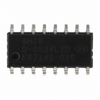
Manufacturer Part Number
FS7140-01G-XTD
Description
IC CLOCK GEN PLL PROGR 16-SOIC
Manufacturer
ON Semiconductor
Type
PLL Clock Generatorr
Datasheet
1.FS7145-01-XTP.pdf
(19 pages)
Specifications of FS7140-01G-XTD
Pll
Yes
Input
Crystal
Output
CMOS, PECL
Number Of Circuits
1
Ratio - Input:output
2:1
Differential - Input:output
No/Yes
Frequency - Max
400MHz
Divider/multiplier
Yes/No
Voltage - Supply
3 V ~ 3.6 V
Operating Temperature
0°C ~ 70°C
Mounting Type
Surface Mount
Package / Case
16-SOIC (3.9mm Width)
Frequency-max
340MHz
Mounting Style
SMD/SMT
Max Input Freq
80 MHz
Max Output Freq
340 MHz
Number Of Outputs
1
Operating Supply Voltage
3.3 V
Operating Temperature Range
0 C to + 70 C
Supply Current
35 mA
Lead Free Status / RoHS Status
Lead free / RoHS Compliant
Other names
766-1028
Available stocks
Company
Part Number
Manufacturer
Quantity
Price
Company:

Part Number:
FS7140-01G-XTD
Manufacturer:
ON
Quantity:
1 789


FS714x
Table 12: DC Electrical Specifications
Parameter
Overall
Supply current, dynamic
Supply current, static
Serial Communication I/O (SDA, SCL)
High-level input voltage
Low-level input voltage
Hysteresis voltage
Input leakage current
Low-level output sink current (SDA)
Address Select Input (ADDR0, ADDR1)
High-level input voltage
Low-level input voltage
High-level input current (pull-down)
Low-level input current
Reference Frequency Input (REF)
High-level input voltage
Low-level input voltage
High-level input current
Low-level input current (pull-down)
Sync Control Input (SYNC)
High-level input voltage
Low-level input voltage
High-level input current
Low-level input current (pull-down)
Crystal Oscillator Input (XIN)
Threshold bias voltage
High-level input current
Low-level input current
Crystal frequency
Recommended crystal load capacitance*
Crystal Oscillator Output (XOUT)
High-level output source current
Low-level output sink current
PECL Current Program I/O (IPRG)
Low-level input current
Clock Outputs, CMOS Mode (CLKN, CLKP)
High-level output source current
Low-level output sink current
Clock Outputs, PECL Mode (CLKN, CLKP)
IPRG bias voltage
IPRG bias current
Sink current to IPRG current ratio
Tristate output current
Unless otherwise stated, VDD = 3.3V ± 10%, no load on any output, and ambient temperature range T
nominal characterization data and are not production tested to any specific limits. MIN and MAX characterization data are ± 3σ from typical. Negative currents indicate flows
out of the device.
I
V
V
I
V
I
V
V
V
C
V
Symbol
I
V
I
V
I
V
I
I
V
I
I
I
I
F
I
I
I
I
I
I
I
DD
DDL
I
OL
IH
IL
IH
IL
IH
IL
IH
IL
OH
OL
IL
OH
OL
IPRG
Z
X
IH
IL
hys
IH
IL
IH
IL
IH
IL
TH
L(XTAL)
IPRG
Rev. 5 | Page 15 of 19 | www.onsemi.com
Conditions/Description
CMOS mode; F
400MHz; F
load current
SHUT1, SHUT2 bit both “1”
SDA, SCL in read condition
SDA in acknowledge condition; V
V
V
V
V
V
V
V
V
Fundamental mode
For best matching with internal crystal
oscillator load
V
V
V
V
V
V
resistor is connected from VDD to IPRG
I
IPRG
ADDRx
ADDRx
REF
REF
REF
REF
XIN
XIN
XOUT
XOUT
IPRG
O
O
IPRG
= 2.0V
= 0.4V
= V
= GND
– (V
= V
= 0V
= V
= 0V
= 0V; PECL mode
= 0
= V
will be clamped to this level when a
= V
= 0V
DD
DD
DD
VDD
DD
DD
CLK
– V
= 200MHz; does not include
IPRG
XTAL
) / R
SET
= 15MHz; F
SDA
A
= 0°C to 70°C. Parameters denoted with an asterisk (*) represent
= 0.4V
VCO
=
V
V
V
0.8*V
DD
DD
DD
Min.
-10
-10
-10
-1
-1
-1
5
– 1.0
– 1.0
– 1.0
DD
0.33*V
16-18
V
V
Typ.
400
-8.5
-30
-30
-40
-35
35
14
30
40
11
19
13
DD
DD
/2
/3
DD
0.2*V
Max.
700
+10
0.8
0.8
0.8
3.5
35
10
10
1
1
1
DD
Units
MHz
mA
mA
mA
mA
mA
mA
mA
µA
µA
µA
µA
µA
µA
µA
µA
µA
µA
µA
µA
pF
V
V
V
V
V
V
V
V
V
V
V
Related parts for FS7140-01G-XTD
Image
Part Number
Description
Manufacturer
Datasheet
Request
R

Part Number:
Description:
IC CLOCK GEN PLL PROGR 16-SSOP
Manufacturer:
ON Semiconductor
Datasheet:

Part Number:
Description:
IC CLOCK GEN PLL PROG 16SOIC
Manufacturer:
ON Semiconductor
Datasheet:
Part Number:
Description:
IC CLOCK GEN PLL PROG 16SSOP
Manufacturer:
ON Semiconductor
Datasheet:
Part Number:
Description:
Programmable Phase- Locked Loop Clock Generator
Manufacturer:
ON Semiconductor
Datasheet:

Part Number:
Description:
Programmable Phase-Locked Loop Clock Generator
Manufacturer:
AMI [AMI SEMICONDUCTOR]
Datasheet:
Part Number:
Description:
ON Semiconductor [VOLTAGE REGULATOR]
Manufacturer:
ON Semiconductor
Datasheet:
Part Number:
Description:
357-036-542-201 CARDEDGE 36POS DL .156 BLK LOPRO
Manufacturer:
ON Semiconductor
Datasheet:
Part Number:
Description:
357-036-542-201 CARDEDGE 36POS DL .156 BLK LOPRO
Manufacturer:
ON Semiconductor
Datasheet:
Part Number:
Description:
357-036-542-201 CARDEDGE 36POS DL .156 BLK LOPRO
Manufacturer:
ON Semiconductor
Datasheet:
Part Number:
Description:
357-036-542-201 CARDEDGE 36POS DL .156 BLK LOPRO
Manufacturer:
ON Semiconductor
Datasheet:
Part Number:
Description:
357-036-542-201 CARDEDGE 36POS DL .156 BLK LOPRO
Manufacturer:
ON Semiconductor
Datasheet:
Part Number:
Description:
357-036-542-201 CARDEDGE 36POS DL .156 BLK LOPRO
Manufacturer:
ON Semiconductor
Datasheet:
Part Number:
Description:
357-036-542-201 CARDEDGE 36POS DL .156 BLK LOPRO
Manufacturer:
ON Semiconductor
Datasheet:
Part Number:
Description:
357-036-542-201 CARDEDGE 36POS DL .156 BLK LOPRO
Manufacturer:
ON Semiconductor
Datasheet:
Part Number:
Description:
357-036-542-201 CARDEDGE 36POS DL .156 BLK LOPRO
Manufacturer:
ON Semiconductor
Datasheet: