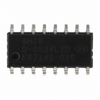
FS7140-01G-XTD ON Semiconductor, FS7140-01G-XTD Datasheet - Page 5

FS7140-01G-XTD
Manufacturer Part Number
FS7140-01G-XTD
Description
IC CLOCK GEN PLL PROGR 16-SOIC
Manufacturer
ON Semiconductor
Type
PLL Clock Generatorr
Datasheet
1.FS7145-01-XTP.pdf
(19 pages)
Specifications of FS7140-01G-XTD
Pll
Yes
Input
Crystal
Output
CMOS, PECL
Number Of Circuits
1
Ratio - Input:output
2:1
Differential - Input:output
No/Yes
Frequency - Max
400MHz
Divider/multiplier
Yes/No
Voltage - Supply
3 V ~ 3.6 V
Operating Temperature
0°C ~ 70°C
Mounting Type
Surface Mount
Package / Case
16-SOIC (3.9mm Width)
Frequency-max
340MHz
Mounting Style
SMD/SMT
Max Input Freq
80 MHz
Max Output Freq
340 MHz
Number Of Outputs
1
Operating Supply Voltage
3.3 V
Operating Temperature Range
0 C to + 70 C
Supply Current
35 mA
Lead Free Status / RoHS Status
Lead free / RoHS Compliant
Other names
766-1028
Available stocks
Company
Part Number
Manufacturer
Quantity
Price
Company:
Part Number:
FS7140-01G-XTD
Manufacturer:
ON
Quantity:
1 789
FS714x
When not using the REF input, it is preferred to leave it floating or connected to V
4.1.6. Feedback Divider Source MUX
The source of frequency for the feedback divider may be selected to be either the output of the post divider or the output of the VCO by
the FBKDSRC bit.
Ordinarily, for frequency synthesis, the output of the VCO is used. Use the output of the post divider only where a deterministic phase
relationship between the output clock and reference clock are desired (line-locked mode, for example).
4.1.7. Device Shutdown
Two bits are provided to effect shutdown of the device if desired, when it is not active. SHUT1 disables most externally observable
device functions. SHUT2 reduces device quiescent current to absolute minimum values. Normally, both bits should be set or cleared
together.
Serial communications capability is not disabled by either SHUT1 or SHUT2.
4.2 Differential Output Stage
The differential output stage supports both CMOS and pseudo-ECL (PECL) signals. The desired output interface is chosen via the
programming registers.
If a PECL interface is used, the transmission line is usually terminated using a Thévenin termination. The output stage can only sink
current in the PECL mode, and the amount of sink current is set by a programming resistor on the LOCK/IPRG pin. The ratio of output
sink current to IPRG current is 13:1. Source current for the CLKx pins is provided by the pull-up resistors that are part of the Thévenin
termination.
4.2.1. Example
Assume that it is desired to connect a PECL-type fanout buffer right next to the FS7140.
Further assume:
• V
• Desired V
• Desired V
• Equivalent R
DD
= 3.3V
HI
LO
= 2.4V
= 1.6V
LOAD
= 75 ohms
Rev. 5 | Page 5 of 19 | www.onsemi.com
DD
.


