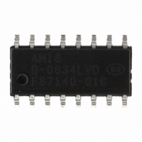
FS7140-01G-XTD ON Semiconductor, FS7140-01G-XTD Datasheet - Page 7

FS7140-01G-XTD
Manufacturer Part Number
FS7140-01G-XTD
Description
IC CLOCK GEN PLL PROGR 16-SOIC
Manufacturer
ON Semiconductor
Type
PLL Clock Generatorr
Datasheet
1.FS7145-01-XTP.pdf
(19 pages)
Specifications of FS7140-01G-XTD
Pll
Yes
Input
Crystal
Output
CMOS, PECL
Number Of Circuits
1
Ratio - Input:output
2:1
Differential - Input:output
No/Yes
Frequency - Max
400MHz
Divider/multiplier
Yes/No
Voltage - Supply
3 V ~ 3.6 V
Operating Temperature
0°C ~ 70°C
Mounting Type
Surface Mount
Package / Case
16-SOIC (3.9mm Width)
Frequency-max
340MHz
Mounting Style
SMD/SMT
Max Input Freq
80 MHz
Max Output Freq
340 MHz
Number Of Outputs
1
Operating Supply Voltage
3.3 V
Operating Temperature Range
0 C to + 70 C
Supply Current
35 mA
Lead Free Status / RoHS Status
Lead free / RoHS Compliant
Other names
766-1028
Available stocks
Company
Part Number
Manufacturer
Quantity
Price
Company:
Part Number:
FS7140-01G-XTD
Manufacturer:
ON
Quantity:
1 789
FS714x
5.1.3. STOP Data Transfer
A low to high transition of the SDA line while SCL input is high indicates a STOP condition. All commands to the device must be
followed by a STOP condition.
5.1.4. Data Valid
The state of the SDA line represents valid data if the SDA line is stable for the duration of the high period of the SCL line after a START
condition occurs. The data on the SDA line must be changed only during the low period of the SCL signal. There is one clock pulse per
data bit.
Each data transfer is initiated by a START condition and terminated with a STOP condition. The number of data bytes transferred
between START and STOP conditions is determined by the master device, and can continue indefinitely. However, data that is
overwritten to the device after the first eight bytes will overflow into the first register, then the second, and so on, in a first-in, first-
overwritten fashion.
5.1.5. Acknowledge
When addressed, the receiving device is required to generate an acknowledge after each byte is received. The master device must
generate an extra clock pulse to coincide with the acknowledge bit. The acknowledging device must pull the SDA line low during the
high period of the master acknowledge clock pulse. Setup and hold times must be taken into account.
The master must signal an end of data to the slave by not generating and acknowledge bit on the last byte that has been read (clocked)
out of the slave. In this case, the slave must leave the SDA line high to enable the master to generate a STOP condition.
5.2 I
All programmable registers can be accessed randomly or sequentially via this bi-directional two wire digital interface. The crystal
oscillator does not have to run for communication to occur.
The device accepts the following I
5.2.1. Slave Address
After generating a START condition, the bus master broadcasts a seven-bit slave address followed by a R/W bit. The address of the
device is:
A6
1
where X is controlled by the logic level at the ADDR pins. The selectable ADDR bits allow four different FS7140 devices to exist on the
same bus. Note that every device on an I
5.2.2. Random Register Write Procedure
Random write operations allow the master to directly write to any register. To initiate a write procedure, the R/W bit that is transmitted
after the seven-bit device address is a logic-low. This indicates to the addressed slave device that a register address will follow after the
slave device acknowledges its device address. The register address is written into the slave's address pointer. Following an
acknowledge by the slave, the master is allowed to write eight bits of data into the addressed register. A final acknowledge is returned
by the device, and the master generates a STOP condition.
If either a STOP or a repeated START condition occurs during a register write, the data that has been transferred is ignored.
2
C-bus Operation
A5
0
2
C-bus commands:
A4
1
2
C-bus must have a unique address to avoid possible bus conflicts.
Rev. 5 | Page 7 of 19 | www.onsemi.com
A3
1
A2
0
A1
X
A0
X


