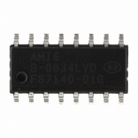
FS7140-01G-XTD ON Semiconductor, FS7140-01G-XTD Datasheet

FS7140-01G-XTD
Specifications of FS7140-01G-XTD
Available stocks
Related parts for FS7140-01G-XTD
FS7140-01G-XTD Summary of contents
Page 1
... Very low “cumulative” jitter 2.0 Description The FS714x (FS7140x or FS7145x monolithic CMOS clock generator/regenerator IC designed to minimize cost and component count in a variety of electronic systems. Via the I The length of the reference and feedback dividers, their fine granularity and the flexibility of the post divider make the FS714x the most flexible stand-alone PLL clock generator available ...
Page 2
... FS714x Table 1: FS7140 Pin Descriptions Pin Type Name Description 1 DI SCL Serial interface clock (requires an external pull-up) 2 DIO SDA Serial interface data input/output (requires an external pull-up ADDR0 Address select bit “0” VSS Ground 5 AI XIN Crystal oscillator feedback 6 AO XOUT ...
Page 3
FS714x Table 2: FS7145 Pin Descriptions Pin Type Name Description 1 DI SCL Serial interface clock (requires an external pull-up) 2 DIO SDA Serial interface data input/output (requires an external pull-up ADDR0 Address select bit “0” ...
Page 4
... See Table 8 for additional information. 4.1.4. Crystal Oscillator The FS7140 is equipped with a Pierce-type crystal oscillator. The crystal is operated in parallel resonant mode. Internal load capacitance is provided for the crystal. While a recommended load capacitance for the crystal is specified, crystals for other standard load capacitances may be used if great precision of the reference frequency (100ppm or less) is not required. ...
Page 5
... PECL mode, and the amount of sink current is set by a programming resistor on the LOCK/IPRG pin. The ratio of output sink current to IPRG current is 13:1. Source current for the CLKx pins is provided by the pull-up resistors that are part of the Thévenin termination. 4.2.1. Example Assume that it is desired to connect a PECL-type fanout buffer right next to the FS7140. Further assume: • 3.3V DD • ...
Page 6
FS714x Then: R1 (from CLKP and CLKN output to VDD LOAD 3.3 / 2.4 = 103 ohms R2 (from CLKP and CLKN output to GND ...
Page 7
... where X is controlled by the logic level at the ADDR pins. The selectable ADDR bits allow four different FS7140 devices to exist on the same bus. Note that every device 5.2.2. Random Register Write Procedure Random write operations allow the master to directly write to any register. To initiate a write procedure, the R/W bit that is transmitted after the seven-bit device address is a logic-low ...
Page 8
FS714x 5.2.3. Random Register Read Procedure Random read operations allow the master to directly read from any register. To perform a read procedure, the R/W bit that is transmitted after the seven-bit address is a logic-low the register ...
Page 9
FS714x Figure 4: Random Register Write Procedure Figure 5: Random Register Read Procedure Figure 6: Sequential Register Write Procedure Rev Page www.onsemi.com ...
Page 10
FS714x Figure 7: Sequential Register Read Procedure Rev Page www.onsemi.com ...
Page 11
... FS714x 6.0 Programming Information All register bits are cleared to zero on power-up. All register bits may be read back as written. Table 3: FS7140 Register Map Address BIT 7 BIT 6 Reserved Reserved Byte 7 (Bit 63) (Bit 62) Must be set to “0” Must be set to “0” Reserved Reserved (Bit 55) ...
Page 12
FS714x Table 4: FS7145 Register Map Address BIT 7 BIT 6 Reserved Reserved Byte 7 (Bit 63) (Bit 62) Must be set to “0” Must be set to “0” Reserved Reserved (Bit 55) (Bit 54) Byte 6 Must be set ...
Page 13
FS714x Table 8: SYNC Control Bits (FS7145 only) Name Description SYNCEN Sync enable [0] = disabled / [1] = enabled SYNCPOL Sync polarity [0] = negative edge / [1] = positive edge Table 9: Post Divider Control Bits Name Description ...
Page 14
FS714x 7.0 Electrical Specifications Table 10: Absolute Maximum Ratings Parameter Supply voltage ground) SS Input voltage, dc Output voltage, dc Input clamp current < > Output clamp current, ...
Page 15
FS714x Table 12: DC Electrical Specifications Parameter Overall Supply current, dynamic Supply current, static Serial Communication I/O (SDA, SCL) High-level input voltage Low-level input voltage Hysteresis voltage Input leakage current Low-level output sink current (SDA) Address Select Input (ADDR0, ADDR1) ...
Page 16
FS714x Table 13: AC Timing Specifications Parameter Symbol Overall Output frequency* f o(max) VCO frequency* f VCO CMOS mode rise time CMOS mode fall time PECL mode rise time PECL mode fall time* t ...
Page 17
FS714x Figure 8: Bus Timing Data Figure 9: Data Transfer Sequence Rev Page www.onsemi.com ...
Page 18
FS714x 8.0 Package Information for ‘Green’ and ‘Non-Green’ Table 15: 16-pin SOIC (0.150") Package Dimensions Dimensions Inches Millimeters Min. Max. Min. Max. A 0.061 0.068 1.55 1.73 A1 0.004 0.0098 0.102 0.249 A2 0.055 0.061 1.40 1.55 B 0.013 0.019 ...
Page 19
... SOIC FS7140-02G-XTD 16-pin (5.3mm) SSOP ‘Green’ or lead-free packaging 16-pin (5.3mm) SSOP FS7140-02G-XTP ‘Green’ or lead-free packaging FS7140-01G-XTD 16-pin (0.150”) SOIC ‘Green’ or lead-free packaging FS7140-01G-XTP 16-pin (0.150”) SOIC ‘Green’ or lead-free packaging 10.0 Revision History ...


