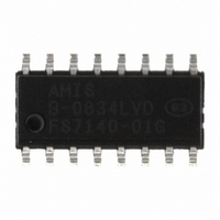
FS7140-01G-XTD ON Semiconductor, FS7140-01G-XTD Datasheet - Page 16

FS7140-01G-XTD
Manufacturer Part Number
FS7140-01G-XTD
Description
IC CLOCK GEN PLL PROGR 16-SOIC
Manufacturer
ON Semiconductor
Type
PLL Clock Generatorr
Datasheet
1.FS7145-01-XTP.pdf
(19 pages)
Specifications of FS7140-01G-XTD
Pll
Yes
Input
Crystal
Output
CMOS, PECL
Number Of Circuits
1
Ratio - Input:output
2:1
Differential - Input:output
No/Yes
Frequency - Max
400MHz
Divider/multiplier
Yes/No
Voltage - Supply
3 V ~ 3.6 V
Operating Temperature
0°C ~ 70°C
Mounting Type
Surface Mount
Package / Case
16-SOIC (3.9mm Width)
Frequency-max
340MHz
Mounting Style
SMD/SMT
Max Input Freq
80 MHz
Max Output Freq
340 MHz
Number Of Outputs
1
Operating Supply Voltage
3.3 V
Operating Temperature Range
0 C to + 70 C
Supply Current
35 mA
Lead Free Status / RoHS Status
Lead free / RoHS Compliant
Other names
766-1028
Available stocks
Company
Part Number
Manufacturer
Quantity
Price
Company:
Part Number:
FS7140-01G-XTD
Manufacturer:
ON
Quantity:
1 789
FS714x
Table 13: AC Timing Specifications
Parameter
Overall
Output frequency*
VCO frequency*
CMOS mode rise time*
CMOS mode fall time*
PECL mode rise time*
PECL mode fall time*
Reference Frequency Input (REF)
Input frequency
Reference high time
Reference low time
Sync Control Input (SYNC)
Sync high time
Sync low time
Clock Output (CLKP, CLKN)
Duty cycle (CMOS mode)*
Duty cycle (PECL mode)*
Jitter, long term (σ
Jitter, period (peak-peak)*
Unless otherwise stated, V
nominal characterization data and are not production tested to any specific limits. MIN and MAX characterization data are ± 3σ from typical.
Table 14: Serial Interface Timing Specifications
Parameter
Clock frequency
Bus free time between STOP and START
Set-up time, START (repeated)
Hold time, START
Set-up time, data input
Hold time, data input
Output data valid from clock
Rise time, data and clock
Fall time, data and clock
High time, clock
Low time, clock
Set-up time, STOP
Unless otherwise stated, V
nominal characterization data and are not production tested to any specific limits. MIN and MAX characterization data are ± 3σ from typical.
y
(τ))*
DD
DD
= 3.3V ± 10%, no load on any output, and ambient temperature range T
= 3.3V ± 10%, no load on any output, and ambient temperature range T
Symbol
f
f
t
t
t
t
F
t
t
t
t
t
t
o(max)
VCO
r
f
r
f
REHF
REFL
SYNCH
SYNCL
j(LT)
j(ΔP)
REF
Measured at 1.4V
Conditions/Description
CMOS outputs
PECL outputs
C
C
C
C
For orderly CLK stop/start
For orderly CLK stop/start
Measured at zero crossings of (V
For valid programming solutions. Long-term (or cumulative) jitter specified is RMS
position error of any edge compared with an ideal clock generated from the same
reference frequency. It is measured with a time interval analyzer using a 500
microsecond window, using statistics gathered over 1000 samples.
FREF/NREF > 1000kHz
FREF/NREF ~= 500kHz
FREF/NREF ~= 250kHz
FREF/NREF ~= 125kHz
FREF/NREF ~= 62.5kHz
FREF/NREF ~= 31.5kHz
40MHz < VCO frequency <100MHz
VCO frequency > 100MHz
L
L
L
L
Symbol
f
t
T
t
T
t
t
t
t
t
t
T
= 7pF
= 7pF
= 7pF; R
= 7pF; R
SCL
BUF
hd:STA
hd:DAT
AA
R
F
HI
LO
su:STA
su:DAT
su:STO
L
L
Rev. 5 | Page 16 of 19 | www.onsemi.com
= 65 ohm
= 65 ohm
Conditions/Description
SCL
SDA
SDA
SDA, SCL
SDA, SCL
SCL
SCL
CLKP
– V
CLKN
)
A
A
= 0°C to 70°C. Parameters denoted with an asterisk (*) represent
= 0°C to 70°C. Parameters denoted with an asterisk (*) represent
1300
1300
Clock
(MHz)
Min.
600
600
100
600
600
0
0
Fast Mode
Min.
40
Max.
0
0
3
3
3
3
400
900
300
300
Typ.
100
190
240
300
50
50
25
50
75
50
1
1
1
1
Max.
150
300
400
80
Units
kHz
ns
ns
ns
ns
ns
ns
ns
ns
ns
ns
ns
Units
MHz
MHz
MHz
T
T
ns
ns
ns
ns
ns
ns
ps
ps
ps
ps
ps
ps
ps
ps
ps
%
%
CLK
CLK


