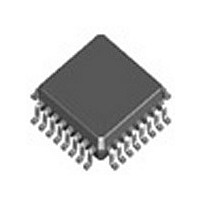
ICS8624BYLF IDT, Integrated Device Technology Inc, ICS8624BYLF Datasheet - Page 12

ICS8624BYLF
Manufacturer Part Number
ICS8624BYLF
Description
IC BUFFER ZD 1-5 HSTL 32-LQFP
Manufacturer
IDT, Integrated Device Technology Inc
Series
HiPerClockS™r
Type
Fanout Distribution, Multiplexer , Zero Delay Bufferr
Datasheet
1.ICS8624BYLFT.pdf
(19 pages)
Specifications of ICS8624BYLF
Pll
Yes with Bypass
Input
HCSL, LVDS, LVHSTL, LVPECL, SSTL
Output
HSTL
Number Of Circuits
1
Ratio - Input:output
2:5
Differential - Input:output
Yes/Yes
Frequency - Max
700MHz
Divider/multiplier
Yes/No
Voltage - Supply
3.135 V ~ 3.465 V
Operating Temperature
0°C ~ 70°C
Mounting Type
Surface Mount
Package / Case
32-LQFP
Frequency-max
700MHz
Number Of Elements
1
Supply Current
120mA
Pll Input Freq (min)
31.25MHz
Pll Input Freq (max)
700MHz
Operating Supply Voltage (typ)
3.3V
Operating Temp Range
0C to 70C
Package Type
LQFP
Output Frequency Range
Up to 700MHz
Operating Supply Voltage (min)
3.135V
Operating Supply Voltage (max)
3.465V
Operating Temperature Classification
Commercial
Pin Count
32
Lead Free Status / RoHS Status
Lead free / RoHS Compliant
Other names
8624BYLF
Available stocks
Company
Part Number
Manufacturer
Quantity
Price
Company:
Part Number:
ICS8624BYLF
Manufacturer:
IDT, Integrated Device Technology Inc
Quantity:
10 000
Part Number:
ICS8624BYLF
Manufacturer:
ICS
Quantity:
20 000
Company:
Part Number:
ICS8624BYLFT
Manufacturer:
IDT, Integrated Device Technology Inc
Quantity:
10 000
ICS8624 Data Sheet
The following component footprints are used in this layout example:
All the resistors and capacitors are size 0603.
Power and Grounding
Place the decoupling capacitors C1, C6, C2, C4, and C5, as close as
possible to the power pins. If space allows, placement of the
decoupling capacitor on the component side is preferred. This can
reduce unwanted inductance between the decoupling capacitor and
the power pin caused by the via.
Maximize the power and ground pad sizes and number of vias
capacitors. This can reduce the inductance between the power and
ground planes and the component power and ground pins.
The RC filter consisting of R7, C11, and C16 should be placed as
close to the V
Clock Traces and Termination
Poor signal integrity can degrade the system performance or cause
system failure. In synchronous high-speed digital systems, the clock
signal is less tolerant to poor signal integrity than other signals. Any
ringing on the rising or falling edge or excessive ring back can cause
system failure. The shape of the trace and the trace delay might be
restricted by the available space on the board and the component
Figure 4B. PCB Board Layout for ICS8624
ICS8624BY REVISION E OCTOBER 6, 2009
U1
Pin 1
DDA
C1
C6
pin as possible.
R7
C16
C11
C7
C2
C5
C4
12
location. While routing the traces, the clock signal traces should be
routed first and should be locked prior to routing other signal traces.
The matching termination resistors should be located as close to the
receiver input pins as possible.
• The differential 50Ω output traces should have same length.
• Avoid sharp angles on the clock trace. Sharp angle turns
• Keep the clock traces on the same layer. Whenever possible,
• To prevent cross talk, avoid routing other signal traces in
• Make sure no other signal traces are routed between the
cause the characteristic impedance to change on the
transmission lines.
avoid placing vias on the clock traces. Placement of vias on
the traces can affect the trace characteristic impedance and
hence degrade signal integrity.
parallel with the clock traces. If running parallel traces is
unavoidable, allow a separation of at least three trace widths
between the differential clock trace and the other signal trace.
clock trace pair.
LOW SKEW, 1-TO-5 DIFFERENTIAL-TO-HSTL ZERO DELAY BUFFER
GND
50 Ohm
Traces
VDDO
VDD
VDDA
VIA
©2009 Integrated Device Technology, Inc.


