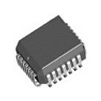
IDT74FCT388915TDJG8 IDT, Integrated Device Technology Inc, IDT74FCT388915TDJG8 Datasheet - Page 9

IDT74FCT388915TDJG8
Manufacturer Part Number
IDT74FCT388915TDJG8
Description
IC PLL CLK GENERATOR 3ST 28-PLCC
Manufacturer
IDT, Integrated Device Technology Inc
Series
74FCTr
Type
PLL Clock Driverr
Datasheet
1.IDT74FCT388915TBJG8.pdf
(10 pages)
Specifications of IDT74FCT388915TDJG8
Pll
Yes with Bypass
Input
LVTTL
Output
LVCMOS, LVTTL
Number Of Circuits
1
Ratio - Input:output
2:8
Differential - Input:output
No/No
Frequency - Max
133MHz
Divider/multiplier
Yes/Yes
Voltage - Supply
3 V ~ 3.6 V
Operating Temperature
0°C ~ 70°C
Mounting Type
Surface Mount
Package / Case
28-PLCC
Frequency-max
133MHz
Number Of Elements
1
Pll Input Freq (min)
10MHz
Pll Input Freq (max)
133MHz
Operating Supply Voltage (typ)
3.3V
Operating Temp Range
0C to 70C
Package Type
PLCC
Output Frequency Range
10 to 133MHz
Operating Supply Voltage (min)
3V
Operating Supply Voltage (max)
3.6V
Operating Temperature Classification
Commercial
Pin Count
28
Lead Free Status / RoHS Status
Lead free / RoHS Compliant
Other names
74FCT388915TDJG8
Available stocks
Company
Part Number
Manufacturer
Quantity
Price
Company:
Part Number:
IDT74FCT388915TDJG8
Manufacturer:
IDT, Integrated Device Technology Inc
Quantity:
10 000
TEST CIRCUITS AND WAVEFORMS
NOTES:
1. The FCT388915T aligns rising edges of the FEEDBACK input and SYNC input, therefore the SYNC input does not require a 50% duty cycle.
2. All skew specs are measured between the V
3. If a Q ouput is connected to the FEEDBACK input (this situation is not shown), the Q output frequency would match the SYNC input frequency, the 2Q output would run at twice
NOTES:
1. Diagram shown for input Control Enable-LOW and input Control Disable-HIGH.
2. Pulse Generator for All Pulses: t
Q/2 OUTPUT
IDT74FCT388915T
3.3V LOW SKEW PLL-BASED CMOS CLOCK DRIVER (3-STATE)
Q5 OUTPUT
SYNC IN PUT
(SYNC (1) or
SYNC (0))
2Q OUTPUT
FEED BAC K
INPUT
NORMALLY
NORMALLY
the SYNC frequency and the Q/2 output would run at half the SYNC frequency.
t
Q0-Q4
OUTPUTS
SKEW ALL
CONTROL
OUTPUT
OUTPUT
Generator
Pulse
INPUT
HIGH
LOW
SW ITCH
SW ITCH
GND
ENABLE
(These waveforms represent the configuration of Figure 3a)
V
IN
t
t
6V
PZH
PZL
R
Enable and Disable Times
T
50 Ω Ω Ω Ω Ω to V
Propagation Delay, Output Skew
t
P D
D.U.T.
1.5V
1.5V
3V
0V
t
V
SKEW f
C C
F
t
≤ 2.5ns; t
PHZ
CC
t
CYCLE
D ISABLE
/2, C
t
V
PLZ
OU T
t
CC
R
SKEW r
L
SYNC IN PUT
≤ 2.5ns.
/2 crossing point of the appropriate output edges. All skews are specified as "windows", not as ± deviation around a center point.
= 20pF
0.3V
0.3V
V
CC
t
100
100
CYCLE
V
V
3V
1.5V
0V
3V
0V
OL
O H
Ω
Ω
t
"Q" OUTPUTS
SKEW f
20pF
C
L
9
t
SWITCH POSITION
DEFINITIONS:
C
R
SKEW r
1.5V
L
T
V
V
V
V
V
CC/2
CC/2
CC/2
CC/2
CC/2
= Load capacitance: includes jig and probe capacitance.
= Termination resistance: should be equal to Z
Generator
Pulse
Disable High
Disable Low
Enable High
Enable Low
Test
V
IN
Enable and Disable Test Circuit
R
T
D.U.T.
V
COMMERCIAL TEMPERATURE RANGE
C C
V
OU T
OUT
of the Pulse Generator.
500
500
Switch
Ω
Ω
GND
6V
6.0V
GND


