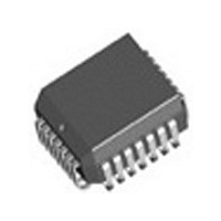
IDT74FCT388915TDJG8 IDT, Integrated Device Technology Inc, IDT74FCT388915TDJG8 Datasheet - Page 4

IDT74FCT388915TDJG8
Manufacturer Part Number
IDT74FCT388915TDJG8
Description
IC PLL CLK GENERATOR 3ST 28-PLCC
Manufacturer
IDT, Integrated Device Technology Inc
Series
74FCTr
Type
PLL Clock Driverr
Datasheet
1.IDT74FCT388915TBJG8.pdf
(10 pages)
Specifications of IDT74FCT388915TDJG8
Pll
Yes with Bypass
Input
LVTTL
Output
LVCMOS, LVTTL
Number Of Circuits
1
Ratio - Input:output
2:8
Differential - Input:output
No/No
Frequency - Max
133MHz
Divider/multiplier
Yes/Yes
Voltage - Supply
3 V ~ 3.6 V
Operating Temperature
0°C ~ 70°C
Mounting Type
Surface Mount
Package / Case
28-PLCC
Frequency-max
133MHz
Number Of Elements
1
Pll Input Freq (min)
10MHz
Pll Input Freq (max)
133MHz
Operating Supply Voltage (typ)
3.3V
Operating Temp Range
0C to 70C
Package Type
PLCC
Output Frequency Range
10 to 133MHz
Operating Supply Voltage (min)
3V
Operating Supply Voltage (max)
3.6V
Operating Temperature Classification
Commercial
Pin Count
28
Lead Free Status / RoHS Status
Lead free / RoHS Compliant
Other names
74FCT388915TDJG8
Available stocks
Company
Part Number
Manufacturer
Quantity
Price
Company:
Part Number:
IDT74FCT388915TDJG8
Manufacturer:
IDT, Integrated Device Technology Inc
Quantity:
10 000
POWER SUPPLY CHARACTERISTICS
NOTES:
1. For conditions shown as Max. or Min., use appropriate value specified under Electrical Characteristics for the applicable device type.
2. Typical values are at V
3. Per TTL driven input. All other inputs at V
4. This parameter is not directly testable, but is derived for use in Total Power Supply Calculations. It is derived with Q frequency as the reference.
5. Values for these conditions are examples of the I
6. I
SYNCH INPUT TIMING REQUIRMENTS
NOTES:
1. Note 7 in "General AC Specification Notes" and Figure 3 describes this specification and its actual limits depending on the feedback connection.
2. Maximum operating frequency is guaranteed with the part in a phase locked condition and all outputs loaded.
3. At this frequency, 2Q cannot be used as feedback.
OUTPUT FREQUENCY SPECIFICATIONS
IDT74FCT388915T
3.3V LOW SKEW PLL-BASED CMOS CLOCK DRIVER (3-STATE)
Symbol
Duty Cycle Input Duty Cycle, SYNC Inputs
Frequency Input Frequency, SYNC Inputs
I
I
ΔI
D
N
I
f = 2Q Frequency
I
T
ΔI
Symbol
C
C
CC
CCD
LOAD
I
C
Symbol
CCD
RISE/FALL
H
T
I
CC
PD
= I
= I
C
fQ/2
CC
f2Q
= Number of TTL Inputs at D
= Quiescent Current (I
= Duty Cycle for TTL Inputs High
fQ
QUIESCENT
CC
= Dynamic Current Caused by an Input Transition Pair (HLH or LHL)
= Power Supply Current for a TTL High Input (V
= Dynamic Current due to load.
+ DI
CC
Parameter
Quiescent Power Supply Current
TTL Inputs HIGH
Dynamic Power Supply Current
Power Dissipation Capacitance
Total Power Supply Current
Parameter
Rise/Fall Times, SYNC inputs
(0.8V to 2V)
+ I
D
Parameter
Operating frequency 2Q Output
Operating frequency Q0-Q4, Q5 Outputs
Operating frequency Q/2 Output
H
INPUTS
N
T
+ I
CC
CCD
+ I
CCL
DYNAMIC
= 3.3V, +25°C ambient.
(f) + I
,
I
CCH
H
LOAD
and I
(6)
CCZ
CC
)
or GND.
(4)
CC
formula. These limits are guaranteed but not tested.
25%
Min.
10
IN
V
V
V
All Outputs Open
50% Duty Cycle
V
PLL_EN = 1, LOCK = 1, FEEDBACK = Q4
SYNC frequency = 50MHz. All bits loaded with 15pF
V
PLL_EN = 1, LOCK = 1, FEEDBACK = Q4
SYNC frequency = 50MHz. All bits loaded with 50Ω Thevenin
termination and 20pF
—
CC
IN
CC
CC
CC
(1)
= 3.4V)
= V
= Max.
= Max.
= Max.
= Max.
CC
2Q fmax
–2.1V
Max.
75%
3
Min.
40
20
10
(3)
MHz
Unit
ns
—
Test Conditions
17.5
4
70
70
35
V
V
V
IN
IN
IN
(1)
= V
= V
= GND
CC
CC
100
100
50
25
–0.6V
(3)
Max.
(2)
133
66.7
33.3
133
COMMERCIAL TEMPERATURE RANGE
Min.
(3)
—
—
—
—
—
150
Typ.
37.5
150
75
0.2
15
30
90
2
(3)
(2)
Max.
120
0.3
30
25
60
MHz
MHz
MHz
Unit
MHz
Unit
mA/
µ A
mA
mA
pF


