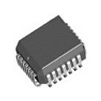
IDT74FCT388915TDJG8 IDT, Integrated Device Technology Inc, IDT74FCT388915TDJG8 Datasheet - Page 8

IDT74FCT388915TDJG8
Manufacturer Part Number
IDT74FCT388915TDJG8
Description
IC PLL CLK GENERATOR 3ST 28-PLCC
Manufacturer
IDT, Integrated Device Technology Inc
Series
74FCTr
Type
PLL Clock Driverr
Datasheet
1.IDT74FCT388915TBJG8.pdf
(10 pages)
Specifications of IDT74FCT388915TDJG8
Pll
Yes with Bypass
Input
LVTTL
Output
LVCMOS, LVTTL
Number Of Circuits
1
Ratio - Input:output
2:8
Differential - Input:output
No/No
Frequency - Max
133MHz
Divider/multiplier
Yes/Yes
Voltage - Supply
3 V ~ 3.6 V
Operating Temperature
0°C ~ 70°C
Mounting Type
Surface Mount
Package / Case
28-PLCC
Frequency-max
133MHz
Number Of Elements
1
Pll Input Freq (min)
10MHz
Pll Input Freq (max)
133MHz
Operating Supply Voltage (typ)
3.3V
Operating Temp Range
0C to 70C
Package Type
PLCC
Output Frequency Range
10 to 133MHz
Operating Supply Voltage (min)
3V
Operating Supply Voltage (max)
3.6V
Operating Temperature Classification
Commercial
Pin Count
28
Lead Free Status / RoHS Status
Lead free / RoHS Compliant
Other names
74FCT388915TDJG8
Available stocks
Company
Part Number
Manufacturer
Quantity
Price
Company:
Part Number:
IDT74FCT388915TDJG8
Manufacturer:
IDT, Integrated Device Technology Inc
Quantity:
10 000
FCT388915T SYSTEM LEVEL TESTING
FUNCTIONALITY
is in low frequency "test mode". In test mode (with FREQ_SEL HIGH), the 2Q
output is inverted from the selected SYNC input, and the Q outputs are divide-
by-2 (negative edge triggered) of the SYNC input, and the Q/2 output is divide-
by-4 (negative edge triggered). With FREQ_SEL LOW the 2Q output is divide-
by-2 of the SYNC, the Q outputs divide-by-4, and the Q/2 output divide-by-8.
IDT74FCT388915T
3.3V LOW SKEW PLL-BASED CMOS CLOCK DRIVER (3-STATE)
When the PLL_EN pin is LOW, the PLL is bypassed and the FCT388915T
CLOCK @ 2f
at point of use
DISTRIBUTE
CLO CK @ f
Figure 4. Multiprocessing Application Using the FCT388915T for Frequency Multiplication
SYSTEM
CLO CK
SO UR CE
CLOCK
@ f
FCT388915T
FCT388915T
PLL
PLL
and Low Board-to-Board skew
2f
2f
FCT388915T
PLL
MEMORY
CAR DS
CMMU
CMMU
CMMU
CMMU
2f
CPU
CPU
8
These relationships can be seen in the block diagram. A recommended test
configuration would be to use SYNC0 or SYNC1 as the test clock input, and tie
PLL_EN and REF_SEL together and connect them to the test select logic.
below, and theFCT 388915T cannot lock onto that low of an input frequency.
In the test mode described above, any test frequency test can be used.
This functionality is needed since most board-level testers run at 1 MHz or
MEMORY
CO NTROL
CM MU
CM MU
CM MU
CM MU
CM MU
CM MU
CLOCK @ 2f
at point of use
CPU
CARD
CPU
CARD
COMMERCIAL TEMPERATURE RANGE


