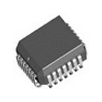
IDT74FCT388915TDJG8 IDT, Integrated Device Technology Inc, IDT74FCT388915TDJG8 Datasheet - Page 5

IDT74FCT388915TDJG8
Manufacturer Part Number
IDT74FCT388915TDJG8
Description
IC PLL CLK GENERATOR 3ST 28-PLCC
Manufacturer
IDT, Integrated Device Technology Inc
Series
74FCTr
Type
PLL Clock Driverr
Datasheet
1.IDT74FCT388915TBJG8.pdf
(10 pages)
Specifications of IDT74FCT388915TDJG8
Pll
Yes with Bypass
Input
LVTTL
Output
LVCMOS, LVTTL
Number Of Circuits
1
Ratio - Input:output
2:8
Differential - Input:output
No/No
Frequency - Max
133MHz
Divider/multiplier
Yes/Yes
Voltage - Supply
3 V ~ 3.6 V
Operating Temperature
0°C ~ 70°C
Mounting Type
Surface Mount
Package / Case
28-PLCC
Frequency-max
133MHz
Number Of Elements
1
Pll Input Freq (min)
10MHz
Pll Input Freq (max)
133MHz
Operating Supply Voltage (typ)
3.3V
Operating Temp Range
0C to 70C
Package Type
PLCC
Output Frequency Range
10 to 133MHz
Operating Supply Voltage (min)
3V
Operating Supply Voltage (max)
3.6V
Operating Temperature Classification
Commercial
Pin Count
28
Lead Free Status / RoHS Status
Lead free / RoHS Compliant
Other names
74FCT388915TDJG8
Available stocks
Company
Part Number
Manufacturer
Quantity
Price
Company:
Part Number:
IDT74FCT388915TDJG8
Manufacturer:
IDT, Integrated Device Technology Inc
Quantity:
10 000
SWITCHING CHARACTERISTICS OVER OPERATING RANGE
GENERAL AC SPECIFICATION NOTES:
1. See test circuit and waveforms.
2. Minimum limits are guaranteed but not tested.
3. These specifications are guaranteed but not production tested.
4. Under equally loaded conditions, as specified under test conditions and at a fixed temperature and voltage.
5. t
6. With V
7. The wiring diagrams and written explanations of Figure 3 demonstrate the input and output frequency relationships for various possible feedback configurations. The allowable
IDT74FCT388915T
3.3V LOW SKEW PLL-BASED CMOS CLOCK DRIVER (3-STATE)
SYNC-FEEDBACK
Q, Q, Q/2 outputs
capacitor shown in Figure 2).
SYNC input range to stay in the phase-locked condition is also indicated. There are two allowable SYNC frequency ranges, depending on whether FREQ_SEL is HIGH or LOW.
Also it is possible to feed back the Q5 output, thus creating a 180° phase shift between the SYNC input and the Q outputs. The table below summarizes the allowable SYNC
frequency range for each possible configuration.
CYCLE
FREQ_SEL
t
PULSE WIDTH (3)
HIGH
HIGH
HIGH
HIGH
Level
t
2Q Output
t
LOW
LOW
LOW
LOW
All Outputs
PULSE WIDTH
SKEW
(falling)
(rising)
t
Symbol
RISE/FALL
t
CC
t
= 1/frequency at which each output (Q, Q, Q/2 or 2Q) is expected to run.
t
LOCK (6)
SKEW
SKEW
t
t
t
t
t
PZH
PHZ
PZL
PLZ
PD
fully powered-on and an output properly connected to the FEEDBACK pin, t
all
(3,4)
(3,4)
r
(3,4)
f
(3)
(3)
Any Q (Q0-Q4)
Any Q (Q0-Q4)
(3)
Feedback
Output
2X_Q
2X_Q
Parameter
Rise/Fall Time
(between 0.8V and 2V)
Output Pulse Width
Q0-Q4, Q5, Q/2, @ 1.5V
Output Pulse Width
SYNC input to FEEDBACK delay
(measured at SYNC0 or 1 and FEEDBACK input pins)
Q/2 (rising edges only)
Output to Output Skew
between outputs Q0-Q4 (falling edges only)
Output to Output Skew
2Q, Q/2, Q0-Q4 rising, Q5 falling
Time required to acquire Phase-Lock from time
SYNC input signal is received
Output Enable Time
Output Disable Time
Output to Output Skew between outputs 2Q, Q0-Q4,
Q/2
Q/2
2Q @ 1.5V
OE/RST (LOW-to-HIGH) to Q, 2Q, Q/2, Q
OE/RST (HIGH-to-LOW) to Q, 2Q, Q/2, Q
Q5
Q5
Frequency Range (MHZ)
10 to (2x_Q f
20 to (2x_Q f
20 to (2x_Q f
10 to (2x_Q f
10 to (2x_Q f
20 to (2x_Q f
Allowable SYNC Input
5 to (2x_Q f
40 to (2x_Q f
MAX
MAX
MAX
MAX
MAX
MAX
MAX
MAX
Spec)/8
Spec)/4
Spec)/2
Spec)/2
Spec)/4
Spec)/4
Spec)/2
Spec)
Corresponding 2Q Output
5
Load = 50Ω to V
Load = 50Ω to V
Load = 50Ω to V
Load = 50Ω to V
LOCK
0.1µF from LF to Analog GND
20 to (2Q f
20 to (2Q f
20 to (2Q f
20 to (2Q f
40 to (2Q f
40 to (2Q f
40 to (2Q f
40 to (2Q f
Frequency Range
Max. is with C1 = 0.1µF, t
Condition
MAX
MAX
MAX
MAX
MAX
MAX
MAX
MAX
Spec)/2
Spec)/2
Spec)/2
Spec)/2
Spec)
Spec)
Spec)
Spec)
CC
CC
CC
CC
/2, C
/2, C
/2, C
/2, C
(1)
L
L
L
L
= 20pF
= 20pF
= 20pF
= 20pF
(5)
LOCK
COMMERCIAL TEMPERATURE RANGE
Min. is with C1 = 0.01µF. (Where C1 is loop filter
0.5t
0.5t
Phase Relationship of the Q Outputs
CYCLE
CYCLE
Min.
0.2
+0.1
3
3
1
—
—
—
(2)
(2)
(2)
(2)
– 0.8
to Rising SYNC Edge
– 1
(5)
(5)
0.5t
0.5t
180°
180°
0°
0°
0°
0°
0°
0°
CYCLE
CYCLE
Max.
+1.3
600
250
800
10
14
14
2
+ 0.8
+ 1
(5)
(5)
Unit
ms
ns
ns
ns
ns
ps
ps
ps
ns
ns


