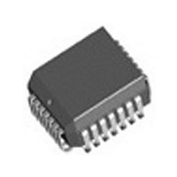
IDT74FCT388915TDJG8 IDT, Integrated Device Technology Inc, IDT74FCT388915TDJG8 Datasheet - Page 6

IDT74FCT388915TDJG8
Manufacturer Part Number
IDT74FCT388915TDJG8
Description
IC PLL CLK GENERATOR 3ST 28-PLCC
Manufacturer
IDT, Integrated Device Technology Inc
Series
74FCTr
Type
PLL Clock Driverr
Datasheet
1.IDT74FCT388915TBJG8.pdf
(10 pages)
Specifications of IDT74FCT388915TDJG8
Pll
Yes with Bypass
Input
LVTTL
Output
LVCMOS, LVTTL
Number Of Circuits
1
Ratio - Input:output
2:8
Differential - Input:output
No/No
Frequency - Max
133MHz
Divider/multiplier
Yes/Yes
Voltage - Supply
3 V ~ 3.6 V
Operating Temperature
0°C ~ 70°C
Mounting Type
Surface Mount
Package / Case
28-PLCC
Frequency-max
133MHz
Number Of Elements
1
Pll Input Freq (min)
10MHz
Pll Input Freq (max)
133MHz
Operating Supply Voltage (typ)
3.3V
Operating Temp Range
0C to 70C
Package Type
PLCC
Output Frequency Range
10 to 133MHz
Operating Supply Voltage (min)
3V
Operating Supply Voltage (max)
3.6V
Operating Temperature Classification
Commercial
Pin Count
28
Lead Free Status / RoHS Status
Lead free / RoHS Compliant
Other names
74FCT388915TDJG8
Available stocks
Company
Part Number
Manufacturer
Quantity
Price
Company:
Part Number:
IDT74FCT388915TDJG8
Manufacturer:
IDT, Integrated Device Technology Inc
Quantity:
10 000
GENERAL AC SPECIFICATION NOTES (continued):
8. The tPD spec describes how the phase offset between the SYNC input and the output connected to the FEEDBACK input, varies with process, temperature and voltage. The
NOTES:
1. Figure 2 shows a loop filter and analog isolation scheme which will be effective in most applications. The following guidelines should be followed to ensure stable and jitter-free
2. In addition to the bypass capacitors used in the analog filter of Figure 2 there should be a 0.1µF bypass capacitor between each of the other (digital) four V
IDT74FCT388915T
3.3V LOW SKEW PLL-BASED CMOS CLOCK DRIVER (3-STATE)
phase measurements were made at 1.5V. The Q/2 output was terminated at the FEEDBACK input with 100Ω to V
the loop filter connection shown in Figure 1 below:
operation:
ground plane. This will reduce output switching noise caused by the 388915T outputs, in addition to reducing potential for noise in the "analog" section of the chip. These bypass
capacitors should also be tied as close to the 388915T package as possible.
a. All loop filter and analog isolation components should be tied as close to the package as possible. Stray current passing through the parasitics of long traces can cause undesirable
b. The 10µF low frequency bypass capacitor and the 0.1µF high frequency bypass capacitor form a wide bandwidth filter that will minimize the 388915T's sensitivity to voltage
c. The loop filter capacitor (0.1µF) can be a ceramic chip capacitor, the same as a standard bypass capacitor.
digital V
that can occur in a high frequency, high speed digital system.
voltage transients at the LF pin.
transients from the system digital V
If good bypass techniques are used on a board design near components which may cause digital V
CC
10
Low
Freq.
Bypass
supply. The purpose of the bypass filtering scheme shown in figure 2 is to give the 388915T additional protection from the power supply and ground plane transients
μ
F
0.1
High
Freq.
Bypass
Figure 2. Recommended Loop Filter and Analog Isolation Scheme for the FCT388915T
μ
F
CC
supply and ground planes.
BOARD V
BOARD GND
External Loop
Filter
0.1
Filter Cap)
CC
μ
F (Loop
Figure 1
0.1
A separate Analog power supply is not necessary
and should not be used. Following these pre-
scribed guidelines is all that is necessary to use
the FCT388915T in a normal digital environm ent.
μ
6
F
LF
Analog GND
C 1
CC
and ground noise, V
ANALOG V
LF
ANALOG GND
CC
Analog loop filter section
of the FCT388915T
and 100Ω to ground. tPD measurements were made with
CC
CC
COMMERCIAL TEMPERATURE RANGE
step deviations should not occur at the 388915T's
CC
pins and the board


