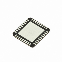
SI5317A-C-GM Silicon Laboratories Inc, SI5317A-C-GM Datasheet - Page 4

SI5317A-C-GM
Manufacturer Part Number
SI5317A-C-GM
Description
IC CLK JITTER CLEANR PROG 36QFN
Manufacturer
Silicon Laboratories Inc
Type
Jitter Cleanerr
Series
Si5317r
Datasheet
1.SI5317C-C-GM.pdf
(46 pages)
Specifications of SI5317A-C-GM
Package / Case
36-QFN
Pll
Yes with Bypass
Input
Clock, Crystal
Output
CML, CMOS, LVDS, LVPECL
Number Of Circuits
1
Ratio - Input:output
1:2
Differential - Input:output
Yes/Yes
Frequency - Max
710MHz
Divider/multiplier
No/No
Voltage - Supply
1.71 V ~ 3.63 V
Operating Temperature
-40°C ~ 85°C
Mounting Type
Surface Mount
Frequency-max
710MHz
Termination Style
SMD/SMT
Output Format
LVPECL
Dimensions
5 mm W x 7 mm L x 1.85 mm H
Minimum Operating Temperature
- 40 C
Maximum Operating Temperature
+ 85 C
Mounting Style
SMD/SMT
Product
XO
Frequency
10 MHz to 945 MHz
Frequency Stability
+/- 20 PPM
Supply Voltage
3.3 Volts
Height
1.85 mm
Lead Free Status / RoHS Status
Lead free / RoHS Compliant
Lead Free Status / RoHS Status
Lead free / RoHS Compliant, Lead free / RoHS Compliant
Other names
336-1923
Si5317
1. Electrical Specifications
Table 1. Recommended Operating Conditions
(V
Table 2. DC Characteristics
(V
4
Temperature Range
Supply Voltage
Note: All minimum and maximum specifications are guaranteed and apply across the recommended operating conditions.
Supply Current (Supply
current is independent of
V
CKIN Input Pin
Input Common Mode
Voltage
(Input Threshold Voltage)
Input Resistance
Input Voltage Level Limits
Single-ended Input Voltage
Swing
Notes:
DD
DD
DD
1. LVPECL outputs require VDD > 2.25 V.
2. This is the amount of leakage that the 3L inputs can tolerate from an external driver. See Figure 3 on page 9. In most
3. No overshoot or undershoot.
)
= 1.8 ±5%, 2.5 ±10%, or 3.3 V ±10%, T
= 1.8 ±5%, 2.5 ±10%, or 3.3 V ±10%, T
Typical values apply at nominal supply voltages and an operating temperature of 25 °C unless otherwise noted.
designs, an external resistor voltage divider is recommended.
Parameter
Parameter
Symbol
V
T
Symbol
DD
CKN
CKN
A
V
V
I
DD
ICM
ISE
RIN
VIN
A
A
= –40 to 85 ºC)
= –40 to 85 ºC)
Test Condition
Only 1 CKOUT Enabled
Only CKOUT1 Enabled
3.3 V nominal
2.5 V nominal
1.8 V nominal
All CKOUTs Enabled
All CKOUTs Enabled
f
f
CKIN
CKIN
622.08 MHz Out
622.08 MHz Out
LVPECL Format
LVPECL Format
Test Condition
19.44 MHz Out
19.44 MHz Out
CMOS Format
CMOS Format
See Figure 2.
See Figure 2.
Single-ended
2.5 V ± 10%
3.3 V ± 10%
Rev. 1.1
1.8 V ± 5%
See note
< 212.5 MHz
> 212.5 MHz
3
1
2
2
1
2.97
2.25
1.71
Min
–40
0.25
Min
0.9
1.0
1.1
0.2
20
—
—
—
—
0
Typ
3.3
2.5
1.8
25
Typ
251
217
204
194
40
—
—
—
—
—
—
Max
1.95
V
279
243
234
220
1.4
1.7
60
—
—
Max
3.63
2.75
1.89
DD
85
Units
V
V
mA
mA
mA
mA
k
Unit
V
V
V
V
PP
PP
ºC
V
V
V


