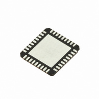
SI5317A-C-GM Silicon Laboratories Inc, SI5317A-C-GM Datasheet - Page 29

SI5317A-C-GM
Manufacturer Part Number
SI5317A-C-GM
Description
IC CLK JITTER CLEANR PROG 36QFN
Manufacturer
Silicon Laboratories Inc
Type
Jitter Cleanerr
Series
Si5317r
Datasheet
1.SI5317C-C-GM.pdf
(46 pages)
Specifications of SI5317A-C-GM
Package / Case
36-QFN
Pll
Yes with Bypass
Input
Clock, Crystal
Output
CML, CMOS, LVDS, LVPECL
Number Of Circuits
1
Ratio - Input:output
1:2
Differential - Input:output
Yes/Yes
Frequency - Max
710MHz
Divider/multiplier
No/No
Voltage - Supply
1.71 V ~ 3.63 V
Operating Temperature
-40°C ~ 85°C
Mounting Type
Surface Mount
Frequency-max
710MHz
Termination Style
SMD/SMT
Output Format
LVPECL
Dimensions
5 mm W x 7 mm L x 1.85 mm H
Minimum Operating Temperature
- 40 C
Maximum Operating Temperature
+ 85 C
Mounting Style
SMD/SMT
Product
XO
Frequency
10 MHz to 945 MHz
Frequency Stability
+/- 20 PPM
Supply Voltage
3.3 Volts
Height
1.85 mm
Lead Free Status / RoHS Status
Lead free / RoHS Compliant
Lead Free Status / RoHS Status
Lead free / RoHS Compliant, Lead free / RoHS Compliant
Other names
336-1923
5. Crystal/Reference Clock Input
The device can use an external crystal or external clock as a reference. If an external clock is used, it must be ac
coupled. With appropriate buffers, the same external reference clock can be applied to CKIN. Although the
reference clock input can be driven single ended (See Figure 14), the best performance is with a crystal or
differential clock source.
External Clock Source
LVPECL, CML, etc.
Figure 16. Differential External Reference Clock Input Example
Figure 15. Sinewave External Reference Clock Input Example
3.3 V
8 mA output current
CMOS buffer,
0 dBm into 50
Figure 14. CMOS External Reference Circuit
For 2.5 V operation, change 130 to 82 .
130
100
50
0.01 F
3.3 V
150
150
Rev. 1.1
0.1 F
0.01 F
0.01 F
0.01 F
0.1 F
0.1 µF
XA
XA
XB
XB
XB
XA
10 pF
Si5317
10 k
Si5317
Si5317
10 k
0.6 V
10 k
10 k
0.6 V
0.6 V
1.2 V
1.2 V
Si5317
29


