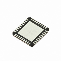
SI5317A-C-GM Silicon Laboratories Inc, SI5317A-C-GM Datasheet - Page 14

SI5317A-C-GM
Manufacturer Part Number
SI5317A-C-GM
Description
IC CLK JITTER CLEANR PROG 36QFN
Manufacturer
Silicon Laboratories Inc
Type
Jitter Cleanerr
Series
Si5317r
Datasheet
1.SI5317C-C-GM.pdf
(46 pages)
Specifications of SI5317A-C-GM
Package / Case
36-QFN
Pll
Yes with Bypass
Input
Clock, Crystal
Output
CML, CMOS, LVDS, LVPECL
Number Of Circuits
1
Ratio - Input:output
1:2
Differential - Input:output
Yes/Yes
Frequency - Max
710MHz
Divider/multiplier
No/No
Voltage - Supply
1.71 V ~ 3.63 V
Operating Temperature
-40°C ~ 85°C
Mounting Type
Surface Mount
Frequency-max
710MHz
Termination Style
SMD/SMT
Output Format
LVPECL
Dimensions
5 mm W x 7 mm L x 1.85 mm H
Minimum Operating Temperature
- 40 C
Maximum Operating Temperature
+ 85 C
Mounting Style
SMD/SMT
Product
XO
Frequency
10 MHz to 945 MHz
Frequency Stability
+/- 20 PPM
Supply Voltage
3.3 Volts
Height
1.85 mm
Lead Free Status / RoHS Status
Lead free / RoHS Compliant
Lead Free Status / RoHS Status
Lead free / RoHS Compliant, Lead free / RoHS Compliant
Other names
336-1923
Si5317
2. Functional Description
2.1. Overview
The Si5317 is a 1:1 jitter-attenuating precision clock for applications requiring sub 1 ps jitter performance. The
Si5317 accepts one clock input ranging from 1 to 711 MHz and generates two clock outputs at the same frequency
ranging from 1 to 711 MHz. The Si5317 is based on Silicon Laboratories' 3rd-generation DSPLL® technology,
which provides jitter attenuation on any frequency in a highly integrated PLL solution that eliminates the need for
external VCXO and loop filter components. The nominal operating frequency is selectable from a look-up table.
The Si5317 PLL loop bandwidth (BW) is selectable via the BWSEL[1:0] pins and supports a range from 60 Hz to
8.4 kHz.
The Si5317 monitors the input clock for loss-of-signal (LOS) and provides a LOS alarm when it detects missing
pulses on the input clock. The device monitors the lock status of the DSPLL. The lock detect algorithm works by
continuously monitoring the phase of the input clock in relation to the phase of the feedback clock.
The Si5317 provides a VCO freeze capability that allows the device to continue generation of a stable output clock
when the selected input clock is lost. During VCO freeze, the DSPLL latches its VCO settings and uses its XA/XB
clock as its frequency reference.
The Si5317 has two output clock drivers and can be configured as four single-ended or two differential outputs.
The signal format of the clock output is selectable to support LVPECL, LVDS, CML, or CMOS loads. The device
operates from a single 1.8, 2.5, or 3.3 V supply. The use of LVPECL requires a VDD > 2.25 V.
14
FRQSEL[3:0]
BWSEL[1:0]
FRQTBL
CKIN+
CKIN–
DEC
LOS
LOL
RST
INC
2
Skew Control
Bandwidth
Frequency
Control
Control
Control
Alarms
Figure 5. Detailed Block Diagram
f
RATE[1:0]
3
External Crystal or
XB
Reference Clock
DSPLL
Rev. 1.1
®
XA
f
OSC
Regulator with
High PSRR
Voltage
2
2
VDD (1.8, 2.5, or 3.3 V)
GND
DBL2_BY
CKOUT+
CKOUT–
SFOUT[1:0]
CKOUT+
CKOUT–


