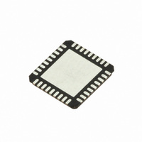
SI5317A-C-GM Silicon Laboratories Inc, SI5317A-C-GM Datasheet - Page 31

SI5317A-C-GM
Manufacturer Part Number
SI5317A-C-GM
Description
IC CLK JITTER CLEANR PROG 36QFN
Manufacturer
Silicon Laboratories Inc
Type
Jitter Cleanerr
Series
Si5317r
Datasheet
1.SI5317C-C-GM.pdf
(46 pages)
Specifications of SI5317A-C-GM
Package / Case
36-QFN
Pll
Yes with Bypass
Input
Clock, Crystal
Output
CML, CMOS, LVDS, LVPECL
Number Of Circuits
1
Ratio - Input:output
1:2
Differential - Input:output
Yes/Yes
Frequency - Max
710MHz
Divider/multiplier
No/No
Voltage - Supply
1.71 V ~ 3.63 V
Operating Temperature
-40°C ~ 85°C
Mounting Type
Surface Mount
Frequency-max
710MHz
Termination Style
SMD/SMT
Output Format
LVPECL
Dimensions
5 mm W x 7 mm L x 1.85 mm H
Minimum Operating Temperature
- 40 C
Maximum Operating Temperature
+ 85 C
Mounting Style
SMD/SMT
Product
XO
Frequency
10 MHz to 945 MHz
Frequency Stability
+/- 20 PPM
Supply Voltage
3.3 Volts
Height
1.85 mm
Lead Free Status / RoHS Status
Lead free / RoHS Compliant
Lead Free Status / RoHS Status
Lead free / RoHS Compliant, Lead free / RoHS Compliant
Other names
336-1923
5.1.3. Jitter Attenuation Performance
The internal VCO uses the XA/XB clock on the XA/XB pins as its reference for jitter attenuation. The XA/XB pins
support either a crystal input or an input buffer single-ended or differential clock input, such that an external
oscillator can become the reference source. In either case, the device accepts a wide margin in absolute frequency
of the XA/XB input (refer to section 3.5.1. "Recovery from VCO Freeze" on page 23). In VCO freeze, the Si5317's
output clock stability matches the clock supplied on the XA/XB pins. The external crystal or clock must be selected
based on the stability requirements of the application if VCO freeze is a key requirement. However, care must be
exercised in certain areas for optimum performance. For examples of connections to the XA/XB pins, refer to
section 5. Figure 22, “Si5317 Typical Application Circuit,” on page 35.
-10
-15
-20
-25
-30
-5
5
0
1
Figure 17. Typical XA-XB Jitter Transfer Function
Jitter Transfer XA/XB Reference to CKOUT
38.88 MHz Clock on XA/XB, RATE[1:0]=LM
10
100
Jitter Frequency (Hz)
Rev. 1.1
1000
10000
100000
1000000
Si5317
31


