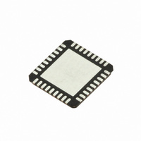
SI5317A-C-GM Silicon Laboratories Inc, SI5317A-C-GM Datasheet - Page 30

SI5317A-C-GM
Manufacturer Part Number
SI5317A-C-GM
Description
IC CLK JITTER CLEANR PROG 36QFN
Manufacturer
Silicon Laboratories Inc
Type
Jitter Cleanerr
Series
Si5317r
Datasheet
1.SI5317C-C-GM.pdf
(46 pages)
Specifications of SI5317A-C-GM
Package / Case
36-QFN
Pll
Yes with Bypass
Input
Clock, Crystal
Output
CML, CMOS, LVDS, LVPECL
Number Of Circuits
1
Ratio - Input:output
1:2
Differential - Input:output
Yes/Yes
Frequency - Max
710MHz
Divider/multiplier
No/No
Voltage - Supply
1.71 V ~ 3.63 V
Operating Temperature
-40°C ~ 85°C
Mounting Type
Surface Mount
Frequency-max
710MHz
Termination Style
SMD/SMT
Output Format
LVPECL
Dimensions
5 mm W x 7 mm L x 1.85 mm H
Minimum Operating Temperature
- 40 C
Maximum Operating Temperature
+ 85 C
Mounting Style
SMD/SMT
Product
XO
Frequency
10 MHz to 945 MHz
Frequency Stability
+/- 20 PPM
Supply Voltage
3.3 Volts
Height
1.85 mm
Lead Free Status / RoHS Status
Lead free / RoHS Compliant
Lead Free Status / RoHS Status
Lead free / RoHS Compliant, Lead free / RoHS Compliant
Other names
336-1923
Si5317
5.1. Crystal/Reference Clock Selection
An external low-jitter clock or a low-cost crystal is used as part of a fixed-frequency oscillator within the DSPLL.
This external clock is required for the device to perform jitter attenuation. Silicon Laboratories recommends using a
high-quality crystal.
In VCO freeze, the DSPLL remains locked to this external clock. Any changes in the frequency of this clock when
the DSPLL is in VCO freeze will be tracked by the output of the device. Note that crystals can have temperature
sensitivities. See “AN591: Crystal Selection for the Si5315 and Si5317“ for a list of approved crystals for the Si5317
and guidance in their selection. AN591 can be downloaded from the Silicon Labs web site: www.silabs.com.
Because the crystal is used as a jitter reference, rapid changes of the crystal temperature can temporarily disturb
the output phase and frequency. For example, it is recommended that the crystal not be placed close to a fan that
is being turned off and on. If a situation such as this is unavoidable, the crystal should be thermally isolated with an
insulating cover.
5.1.1. XA/XB Clock Drift
During VCO freeze, long-term and temperature-related drift of the XA/XB clock input results in a one-to-one drift of
the output frequency. The stability of the any frequency output is identical to the drift of the XA/XB frequency. This
means that for the most demanding applications where the drift of a crystal is not acceptable, an external
temperature-compensated or ovenized oscillator will be required. Drift is not an issue unless the part is in VCO
freeze. Also, the initial accuracy of the XA/XB oscillator (or crystal) is not relevant.
5.1.2. XA/XB Jitter
Jitter on the XA/XB input has a roughly one-to-one transfer function to the output jitter over the bandwidth ranging
from 100 Hz up to 30 kHz. If a crystal is used on the XA/XB pins, this will have low jitter if a suitable crystal is in
use. If the XA/XB pins are connected to an external oscillator, the jitter of the external oscillator may contribute
significantly to the output jitter.
30
*Note: See “AN591: Crystal Selection for the Si5315 and Si5317.”
RATE[1:0]
MM
HM
MH
HH
ML
LM
HL
LH
LL
Fundamental mode crystal*
3rd overtone crystal*
Table 13. XA/XB Reference Sources and Frequencies
External clock
External clock
Reserved
Reserved
Reserved
Reserved
Reserved
Type
Rev. 1.1
Recommended
114.285 MHz
114.285 MHz
38.88 MHz
—
—
—
—
—
—
Lower limit
109 MHz
37 MHz
—
—
—
—
—
—
—
Upper limit
125.5 MHz
41 MHz
—
—
—
—
—
—
—


