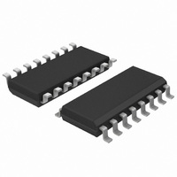
74HCT4046AD,112 NXP Semiconductors, 74HCT4046AD,112 Datasheet - Page 27

74HCT4046AD,112
Manufacturer Part Number
74HCT4046AD,112
Description
IC PHASE LOCK LOOP W/VCO 16SOIC
Manufacturer
NXP Semiconductors
Type
Phase Lock Loop (PLL)r
Series
74HCTr
Datasheet
1.74HCT4046AD112.pdf
(34 pages)
Specifications of 74HCT4046AD,112
Number Of Circuits
1
Package / Case
16-SOIC (3.9mm Width)
Pll
Yes
Input
Clock
Output
Clock
Ratio - Input:output
2:3
Differential - Input:output
No/No
Frequency - Max
19MHz
Divider/multiplier
No/No
Voltage - Supply
4.5 V ~ 5.5 V
Operating Temperature
-40°C ~ 125°C
Mounting Type
Surface Mount
Frequency-max
19MHz
Supply Voltage (max)
5.5 V
Supply Voltage (min)
4.5 V
Maximum Operating Temperature
+ 125 C
Minimum Operating Temperature
- 40 C
Input Level
CMOS
Mounting Style
SMD/SMT
Operating Supply Voltage
4.5 V to 5.5 V
Output Level
CMOS
Lead Free Status / RoHS Status
Lead free / RoHS Compliant
Lead Free Status / RoHS Status
Lead free / RoHS Compliant, Lead free / RoHS Compliant
Other names
568-1547-5
74HCT4046AD
933809570112
74HCT4046AD
933809570112
Philips Semiconductors
1997 Nov 25
SUBJECT
PLL frequency
PLL locks on
noise rejection at
AC ripple content
capture range
signal input
when PLL is
locked
Phase-locked-loop with VCO
harmonics at
centre frequency
PHASE
COMPARATOR
PC1, PC2 or PC3
PC1 or PC3
PC2
PC1
PC2 or PC3
PC1
PC2
PC3
DESIGN CONSIDERATIONS
Loop filter component selection
A small capture range (2f
yes
no
high
low
f
f
f
r
r
r
(a) 1 = R3 x C2; (b) amplitude characteristic (c) pole-zero diagram
= 2f
= f
= f
(a)
i
i
, small ripple content at
, large ripple content at
Fig.28 Simple loop filter for PLL with offset; R3 + R4
i
Fig. 27 Simple loop filter for PLL without offset; R3 500 .
, large ripple content at
2 = R4 x C2;
3 = (R3 + R4) x C2
= R3 x C2 (b) amplitude characteristic (c) pole-zero diagram
27
c
) is obtained if
DEMOUT
DEMOUT
DEMOUT
= 180
= 0
= 90
2f
c
74HC/HCT4046A
1
-- - 2 f
Product specification
L
500 .


