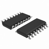
74HCT4046AD,112 NXP Semiconductors, 74HCT4046AD,112 Datasheet - Page 2

74HCT4046AD,112
Manufacturer Part Number
74HCT4046AD,112
Description
IC PHASE LOCK LOOP W/VCO 16SOIC
Manufacturer
NXP Semiconductors
Type
Phase Lock Loop (PLL)r
Series
74HCTr
Datasheet
1.74HCT4046AD112.pdf
(34 pages)
Specifications of 74HCT4046AD,112
Number Of Circuits
1
Package / Case
16-SOIC (3.9mm Width)
Pll
Yes
Input
Clock
Output
Clock
Ratio - Input:output
2:3
Differential - Input:output
No/No
Frequency - Max
19MHz
Divider/multiplier
No/No
Voltage - Supply
4.5 V ~ 5.5 V
Operating Temperature
-40°C ~ 125°C
Mounting Type
Surface Mount
Frequency-max
19MHz
Supply Voltage (max)
5.5 V
Supply Voltage (min)
4.5 V
Maximum Operating Temperature
+ 125 C
Minimum Operating Temperature
- 40 C
Input Level
CMOS
Mounting Style
SMD/SMT
Operating Supply Voltage
4.5 V to 5.5 V
Output Level
CMOS
Lead Free Status / RoHS Status
Lead free / RoHS Compliant
Lead Free Status / RoHS Status
Lead free / RoHS Compliant, Lead free / RoHS Compliant
Other names
568-1547-5
74HCT4046AD
933809570112
74HCT4046AD
933809570112
Philips Semiconductors
FEATURES
GENERAL DESCRIPTION
The 74HC/HCT4046A are high-speed Si-gate CMOS
devices and are pin compatible with the “4046” of the
“4000B” series. They are specified in compliance with
JEDEC standard no. 7A.
The 74HC/HCT4046A are phase-locked-loop circuits that
comprise a linear voltage-controlled oscillator (VCO) and
three different phase comparators (PC1, PC2 and PC3)
with a common signal input amplifier and a common
comparator input.
The signal input can be directly coupled to large voltage
signals, or indirectly coupled (with a series capacitor) to
small voltage signals. A self-bias input circuit keeps small
voltage signals within the linear region of the input
amplifiers. With a passive low-pass filter, the “4046A”
forms a second-order loop PLL. The excellent VCO
linearity is achieved by the use of linear op-amp
techniques.
The VCO requires one external capacitor C1 (between
C1
R
(between R
and capacitor C1 determine the frequency range of the
VCO. Resistor R2 enables the VCO to have a frequency
offset if required.
The high input impedance of the VCO simplifies the design
of low-pass filters by giving the designer a wide choice of
resistor/capacitor ranges. In order not to load the low-pass
filter, a demodulator output of the VCO input voltage is
1997 Nov 25
1
Low power consumption
Centre frequency of up to 17 MHz (typ.) at V
Choice of three phase comparators: EXCLUSIVE-OR;
edge-triggered JK flip-flop;
edge-triggered RS flip-flop
Excellent VCO frequency linearity
VCO-inhibit control for ON/OFF keying and for low
standby power consumption
Minimal frequency drift
Operating power supply voltage range:
VCO section 3.0 to 6.0 V
digital section 2.0 to 6.0 V
Zero voltage offset due to op-amp buffering
Output capability: standard
I
Phase-locked-loop with VCO
CC
A
and GND) or two external resistors R1 and R2
and C1
category: MSI.
1
B
) and one external resistor R1 (between
and GND, and R
2
and GND). Resistor R1
CC
= 4.5 V
2
provided at pin 10 (DEM
techniques where the DEM
voltage lower than the VCO input voltage, here the
DEM
DEM
from DEM
open. The VCO output (VCO
directly to the comparator input (COMP
via a frequency-divider. The VCO output signal has a duty
factor of 50% (maximum expected deviation 1%), if the
VCO input is held at a constant DC level. A LOW level at
the inhibit input (INH) enables the VCO and demodulator,
while a HIGH level turns both off to minimize standby
power consumption.
The only difference between the HC and HCT versions is
the input level specification of the INH input. This input
disables the VCO section. The sections of the comparator
are identical, so that there is no difference in the
SIG
and HCT versions.
Phase comparators
The signal input (SIG
self-biasing amplifier at pin 14, provided that the signal
swing is between the standard HC family input logic levels.
Capacitive coupling is required for signals with smaller
swings.
Phase comparator 1 (PC1)
This is an EXCLUSIVE-OR network. The signal and
comparator input frequencies (f
factor to obtain the maximum locking range. The transfer
characteristic of PC1, assuming ripple (f
suppressed, is:
where V
V
The phase comparator gain is:
The average output voltage from PC1, fed to the VCO
input via the low-pass filter and seen at the demodulator
output at pin 10 (V
differences of signals (SIG
(COMP
equal to
SIG
frequency (f
at f
DEMOUT
o
IN
IN
are shown in Fig.7.
OUT
OUT
(pin 14) or COMP
and with this input the VCO oscillates at the centre
IN
DEMOUT
1
voltage equals that of the VCO input. If
is used, a load resistor (R
) as shown in Fig.6. The average of V
= V
2
OUT
V
o
CC
). Typical waveforms for the PC1 loop locked
PC1OUT
to GND; if unused, DEM
when there is no signal or noise at
V
is the demodulator output at pin 10;
DEMOUT
DEMOUT
(via low-pass filter).
IN
) can be directly coupled to the
IN
OUT
), is the resultant of the phase
(pin 3) inputs between the HC
IN
=
OUT
). In contrast to conventional
) and the comparator input
74HC/HCT4046A
OUT
V
---------- -
K
CC
i
voltage is one threshold
) must have a 50% duty
p
) can be connected
S
=
Product specification
) should be connected
SIGIN
V
---------- - V r ˙ .
OUT
CC
IN
r
), or connected
= 2f
–
should be left
i
COMPIN
) is
DEMOUT
is


