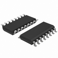
74HCT4046AD,112 NXP Semiconductors, 74HCT4046AD,112 Datasheet - Page 14

74HCT4046AD,112
Manufacturer Part Number
74HCT4046AD,112
Description
IC PHASE LOCK LOOP W/VCO 16SOIC
Manufacturer
NXP Semiconductors
Type
Phase Lock Loop (PLL)r
Series
74HCTr
Datasheet
1.74HCT4046AD112.pdf
(34 pages)
Specifications of 74HCT4046AD,112
Number Of Circuits
1
Package / Case
16-SOIC (3.9mm Width)
Pll
Yes
Input
Clock
Output
Clock
Ratio - Input:output
2:3
Differential - Input:output
No/No
Frequency - Max
19MHz
Divider/multiplier
No/No
Voltage - Supply
4.5 V ~ 5.5 V
Operating Temperature
-40°C ~ 125°C
Mounting Type
Surface Mount
Frequency-max
19MHz
Supply Voltage (max)
5.5 V
Supply Voltage (min)
4.5 V
Maximum Operating Temperature
+ 125 C
Minimum Operating Temperature
- 40 C
Input Level
CMOS
Mounting Style
SMD/SMT
Operating Supply Voltage
4.5 V to 5.5 V
Output Level
CMOS
Lead Free Status / RoHS Status
Lead free / RoHS Compliant
Lead Free Status / RoHS Status
Lead free / RoHS Compliant, Lead free / RoHS Compliant
Other names
568-1547-5
74HCT4046AD
933809570112
74HCT4046AD
933809570112
Philips Semiconductors
VCO section
GND = 0 V; t
DC CHARACTERISTICS FOR 74HCT
Quiescent supply current
Voltages are referenced to GND (ground = 0 V)
Note
1. The value of additional quiescent supply current ( I
1997 Nov 25
SYMBOL PARAMETER
f
SYMBOL PARAMETER
I
INPUT
INH
o
CC
VCO
f/T
f
I
Phase-locked-loop with VCO
VCO
CC
To determine I
frequency stability
VCO centre
frequency (duty
factor = 50%)
VCO frequency
linearity
duty factor at
VCO
quiescent supply
additional quiescent
supply current per
input pin for unit load
coefficient is 1 (note 1)
r
current
V
with temperature
change
(VCO disabled)
= t
I
= V
f
OUT
= 6 ns; C
CC
CC
per input, multiply this value by the unit load coefficient shown in the table below.
2.1 V
L
= 50 pF
7.0
11.0
13.0
min. typ. max. typ. max.
min. typ. max. min. max. min.
10.0
17.0
21.0
1.0
0.4
0.3
50
50
50
+25
100 360
+25
8.0
UNIT LOAD COEFFICIENT
1.00
T
amb
0.20
0.15
0.14
74HC
40 to +85
CC
T
( C)
74HCT
) for a unit load of 1 is given above.
amb
14
40 to +85
( C)
80.0
450
min.
40 to +125
40 to +125
max.
160.0
490
max.
%/K
MHz
%
%
UNIT
UNIT
A
A
3.0
4.5
6.0
3.0
4.5
6.0
3.0
4.5
6.0
3.0
4.5
6.0
V
(V)
74HC/HCT4046A
CC
6.0
4.5
to
5.5
V
TEST CONDITIONS
(V)
CC
TEST CONDITIONS
OTHER
V
R1 = 100 k ; R2 = ;
C1 = 100 pF; see Fig.18
V
R1 = 3 k ; R2 = ;
C1 = 40 pF; see Fig.19
R1 = 100 k ; R2 = ;
C1 = 100 pF;
see Figs 20 and 21
I
VCOIN
= V
Product specification
OTHER
pins 3, 5 and 14
at V
GND; I
pins 3 and 14 to
be excluded
pins 3 and 14
at V
pin 9 at GND;
I
to be excluded
I
VCOIN
at pins 3 and 14
= 1/2 V
CC
CC
; pin 9 at
;
I
= 1/2 V
at
CC
;
CC
;


