SCANSTA111SM National Semiconductor, SCANSTA111SM Datasheet
SCANSTA111SM
Specifications of SCANSTA111SM
Available stocks


Related parts for SCANSTA111SM

SCANSTA111SM Summary of contents
Page 1
... Interrogation Address, Broadcast Address, and 4 Multi- cast Group Addresses (address 000000 is reserved) ■ 3 IEEE 1149.1-compatible configurable local scan ports Connection Diagrams © 2010 National Semiconductor Corporation SCANSTA111 ■ Mode Register selected for insertion into the scan chain individually, or serially in groups of two or three ■ ...
Page 2
LFSR Linear Feedback Shift Register. When enabled, will generate a 16-bit signature of sampled serial test data. LSP Local Scan Port. A four signal port that drives a local (i.e. non-backplane) scan chain. (e.g., TCK TDO , TDI ). 0 ...
Page 3
Architecture Figure 1 shows the basic architecture of the 'STA111. The device's major functional blocks are illustrated here. The TAP Controller, a 16-state state machine, is the central control for the device. The instruction register and various test data reg- ...
Page 4
No. Pin Name Pins I/O VCC 3 N/A 3 N/A GND TMS TDI B TDO TCK B TRST TRIST (B,0- ...
Page 5
No. Pin Name Pins I LOCAL PASS-THROUGH INPUTS: General purpose inputs which can be driven to the backplane A (0-1) pin Y have an internal pull-up resistor LOCAL PASS-THROUGH OUTPUT: General purpose outputs which can be ...
Page 6
The 'STA111 contains three distinct but coupled state-ma- chines (see Figure 2). The first of these is the TAP-control state-machine, which is used to drive the 'STA111's scan ports in conformance with the 1149.1 Standard. The second is the 'STA111-selection ...
Page 7
FIGURE 4. Local SCANSTA111 Port Configuration State Machine The 'STA111's scan port-configuration state-machine is used to control the insertion of local scan ports into the overall scan chain, or the isolation of local ports from the chain. From the perspective ...
Page 8
FIGURE 5. Relationship Between SCANSTA111 State Machines Following a hardware reset, the TAP controller state-machine is in the Test-Logic-Reset (TLR) state; the 'STA111-selection state-machine is in the Wait-For-Address state; and each of the three port-selection state-machines is in the Parked- ...
Page 9
Register Set The SCANSTA111 includes a number of registers which are used for 'STA111 selection and configuration, scan data ma- nipulation, and scan-support operations. These registers can be grouped as shown in Table 3. The specific fields and functions of ...
Page 10
Level 1 Protocol (Addressing Modes) Address Type Hex Address Direct Address 7F. ( (Note Interrogation Address 3A Broadcast Address 3B Multi-Cast Group 0 3C Multi-Cast Group 1 3D Multi-Cast Group 2 3E Multi-Cast ...
Page 11
FIGURE 7. Broadcast Addressing: Address Loaded into Instruction Register FIGURE 8. Multi-Cast Addressing: Address Loaded into Instruction Register 11 10124510 10124511 www.national.com ...
Page 12
Level 2 Protocol Once the SCANSTA111 has been successfully addressed and selected, its internal registers may be accessed via Lev- el-2 Protocol. Level-2 Protocol is compliant to IEEE Std. 1149.1 TAP protocol with one exception: if the 'STA111 is se- ...
Page 13
Instructions Hex Op-Code BYPASS EXTEST SAMPLE/PRELOAD IDCODE UNPARK PARKTLR PARKRTI PARKPAUSE GOTOWAIT (Note 5) MODESEL MODESEL 1 MODESEL 2 MODESEL 3 MCGRSEL SOFTRESET LFSRSEL LFSRON LFSROFF CNTRSEL CNTRON CNTROFF DEFAULT_BYPASS (Note 6) TRANSPARENT0 TRANSPARENT1 TRANSPARENT2 TRANSPARENT3 TRANSPARENT4 TRANSPARENT5 TRANSPARENT6 TRANSPARENT7 ...
Page 14
Instructions Hex Op-Code DGPIO 4 DGPIO 5 DGPIO 6 DGPIO 7 SGPIO 0 SGPIO 1 SGPIO 2 SGPIO 3 SGPIO 4 SGPIO 5 SGPIO 6 SGPIO 7 Other Undefined Note 5: All other instructions act on selected 'STA111s only. Note ...
Page 15
GOTOWAIT: This instruction is used to return all 'STA111s to the Wait-For-Address state. All unparked LSPs will be parked in the Test-Logic-Reset TAP controller state (see ure 5). MODESEL: The MODESEL instruction inserts Mode Regis- ter into the active scan ...
Page 16
FIGURE 10. Local Scan Port Synchronization from Parked-RTI State Register Descriptions INSTRUCTION REGISTER: The instruction shift register is an 8-bit register that is in series with the scan chain whenever the TAP Controller of the SCANSTA111 is in the Shift-IR ...
Page 17
Mode Register(s) Scan Chain Configuration (if unparked) → MR0: X000X000 TDI Register B → MR0: X000X001 TDI Register B → MR0: X000X010 TDI Register B → MR0: X000X011 TDI Register B → MR0: X000X100 TDI Register B → MR0: X000X101 ...
Page 18
Bit status bit for the TCK counter. Bit 7 is only set (logic 1) when the TCK counter is on and has reached terminal count (zero cleared (logic 0) when the counter is loaded following ...
Page 19
Special Features TRANSPARENT MODE While this mode is activated, the selected LSP n ports will follow the backplane ports. TRST is a buffered version of n TRST , TCK is a buffered version of TCK B n buffered version of ...
Page 20
FIGURE 11. Local Scan Port Synchronization on Second Pass FIGURE 12. Synchronization of the Three Local Scan Ports This moves the local chain TAP Controllers to the synchro- nization state (Run-Test/Idle), where they stay until synchro- nization occurs. If the ...
Page 21
Number/Type of GPIO bits: The 'STA111 has both dedicated and shared GPIO (General Purpose I/O). Each dedicated group of GPIO bits supports from dedicated inputs and dedicated outputs. There are provisions for specifying ...
Page 22
UPDATE-DR state and the GPIO input values are written to the corresponding GPIO register during the CAP- TURE-DR state. Dedicated GPIO operation is not supported in the silicon version of the 'STA111. LSP SHARED: In the shared mode ...
Page 23
FIGURE 13. Address Interrogation State Machine 23 10124504 www.national.com ...
Page 24
Absolute Maximum Ratings Supply Voltage ( Input Diode Current ( −0. Input Voltage ( Output Diode Current ( −0. Output Voltage (V ...
Page 25
Symbol Parameter V Maximum Low Output Voltage OL (TRIST , TRIST , LSP_ACTIVE B (0-2) I Maximum Input Leakage Current IN (TCK , (0-6) I Maximum I /Input CCT CC I Maximum Quiescent Supply Current CC I ...
Page 26
Symbol Parameter t , Propagation Delay PHL15 t TMS to TMS PLH15 B (0- Propagation Delay PHL16 t TDI to TDO PLH16 B (0- Enable Time PZL17 TMS PZH17 (0- Disable ...
Page 27
AC Loading and Waveforms FIGURE 14. AC Test Circuit (C AC Waveforms FIGURE 15. Waveforms for an Unparked STA111 in the Shift-DR (IR) TAP Controller State includes probe and jig capacitance 6.0V 50pF 27 10124520 ...
Page 28
Waveform for Inverting and Non-inverting Functions Propagation Delay, Pulse Width and t www.national.com FIGURE 16. Reset Waveforms FIGURE 17. Output Enable Waveforms 10124521 TRI-STATE Output High Enable and Disable Times for Logic TRI-STATE Output Low Enable and Disable Times for ...
Page 29
Capacitance & I/O Characteristics Refer to National's website for IBIS models at http://www.national.com/scan Revision History February, 2010 – Revisions to clarify shared GPIO operation in the silicon version. No specification changes or changes to operation Symbol 2.7 - ...
Page 30
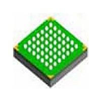
... Physical Dimensions www.national.com inches (millimeters) unless otherwise noted 48-Pin TSSOP NS Package Number MTD48 Ordering Code SCANSTA111MT 49-Pin BGA NS Package Number SLC49a Ordering Code SCANSTA111SM 30 ...
Page 31
Notes 31 www.national.com ...
Page 32
... For more National Semiconductor product information and proven design tools, visit the following Web sites at: www.national.com Products Amplifiers www.national.com/amplifiers Audio www.national.com/audio Clock and Timing www.national.com/timing Data Converters www.national.com/adc Interface www.national.com/interface LVDS www.national.com/lvds Power Management www.national.com/power Switching Regulators www.national.com/switchers LDOs www.national.com/ldo LED Lighting www ...