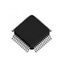
87016AYI IDT, Integrated Device Technology Inc, 87016AYI Datasheet - Page 6

87016AYI
Manufacturer Part Number
87016AYI
Description
Manufacturer
IDT, Integrated Device Technology Inc
Type
Clock Dividerr
Datasheet
1.87016AYI.pdf
(17 pages)
Specifications of 87016AYI
Number Of Clock Inputs
2
Output Frequency
250MHz
Output Logic Level
LVCMOS/LVTTL
Operating Supply Voltage (min)
2.375V
Operating Supply Voltage (typ)
2.5/3.3V
Operating Supply Voltage (max)
3.465V
Package Type
TQFP
Operating Temp Range
-40C to 85C
Operating Temperature Classification
Industrial
Mounting
Surface Mount
Pin Count
48
Lead Free Status / RoHS Status
Not Compliant
AC Electrical Characteristics
Table 5A. AC Characteristics, V
All parameters measured at 250MHz unless noted otherwise.
NOTE 1A: Measured from the V
NOTE 1B: Measured from the differential input crossing point to V
NOTE 2: Defined as skew within a bank with equal load conditions.
NOTE 3: Defined as skew between outputs at the same supply voltage and with equal load conditions. Measured at V
NOTE 4: Defined as skew between outputs on different devices operating a the same supply voltages and with equal load conditions.
Using the same type of input on each device, the output is measured at V
NOTE 5: These parameters are guaranteed by characterization. Not tested in production.
NOTE 6: This parameter is defined in accordance with JEDEC Standard 65.
Table 5B. AC Characteristics, V
For NOTES, please see above, Table 5A.
IDT™ / ICS™ LVCMOS/LVTTL CLOCK GENERATOR
Parameter
f
tp
tsk(b)
tsk(o)
tsk(pp)
t
odc
t
t
Parameter
f
tp
tsk(b)
tsk(o)
tsk(pp)
t
odc
t
t
t
MAX
R
EN
DIS
MAX
R
pw
EN
DIS
ICS87016I
LOW SKEW, 1-TO-16 LVCMOS/LVTTL CLOCK GENERATOR
LH
LH
/ t
/ t
F
F
Symbol
Output Frequency
Propagation Delay,
Low to High
Bank Skew; NOTE 2, 6
Output Skew; NOTE 3, 6
Part-to-Part Skew; NOTE 4, 6
Output Rise/Fall Time; NOTE 5
Output Duty Cycle
Output Enable Time; NOTE 5
Output Disable Time; NOTE 5
Symbol
Output Frequency
Propagation
Delay,
Low to High
Bank Skew; NOTE 2, 6
Output Skew; NOTE 3, 6
Part-to-Part Skew; NOTE 4, 6
Output Rise/Fall Time; NOTE 5
Output Duty Cycle
Output Pulse Width
Output Enable Time; NOTE 5
Output Disable Time; NOTE 5
DD
CLK0; NOTE 1A
CLK1/CLK1;
NOTE 1B
/2 of the input to V
CLK0; NOTE 1A
CLK1/CLK1; NOTE 1B
DD
DD
= V
= V
DDOx
DDOx
= 3.3V ± 5%, T
= 2.5V ± 5%, T
Measured on the Rising Edge
Measured on the Rising Edge
DDOX
/2 of the output.
Test Conditions
20% to 80%
ƒ ≤ 125MHz
ƒ > 125MHz
Measured on the Rising Edge
Measured on the Rising Edge
DDOX
A
A
6
Test Conditions
= -40°C to 85°C
= -40°C to 85°C
/2 of the output.
20% to 80%
ƒ < 175MHz
ƒ ≥ 175MHz
DDOX
/2.
t
Period
Minimum
150
2.9
3.0
40
/2 – 800
Minimum Typical Maximum Units
2.75
200
2.8
45
40
Typical
ICS87016AYI REV. C MAY 25, 2007
3.8
3.6
3.4
3.4
t
Period
Maximum
DDOX
250
210
800
700
4.7
4.3
70
60
/2 + 800
10
10
250
170
800
700
3.9
4.1
50
55
60
10
10
/2.
Units
MHz
MHz
ns
ns
ps
ps
ps
ps
ps
ns
ns
ns
ns
ps
ps
ps
ps
ns
ns
%
%
%


