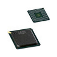
PNX1311EH/G NXP Semiconductors, PNX1311EH/G Datasheet - Page 272

PNX1311EH/G
Manufacturer Part Number
PNX1311EH/G
Description
Manufacturer
NXP Semiconductors
Datasheet
1.PNX1311EHG.pdf
(548 pages)
Specifications of PNX1311EH/G
Lead Free Status / RoHS Status
Compliant
- Current page: 272 of 548
- Download datasheet (6Mb)
PNX1300/01/02/11 Data Book
18.3.3.2
Poll control register to check if output buffer is full. Scan
out data when it is full and clear the ofull control bit. Note
that scanning in any instruction automatically scans out
the 3 least significant bits (including ifull and ofull bits) of
JTAG_CTRL register.
Table 18-4. Transfer of Data out via JTAG
18-6
IR shift in SEL_OFULL_OUT instruction
While JTAG_CTRL.ofull = 0, scan in
DR scan 33 bits of register JTAG_OFULL_OUT
TOTAL
SEL_OFULL_OUT instruction
Transferring data from TriMedia via
JTAG
Action
PRELIMINARY SPECIFICATION
TCK cycles
Number of
61+ cycles
11+
12
38
Note that the above timings do not include the over-
heads of the JTAG software driver for JTAG interface
module plugged into a PC.
18.3.4
It is expected that the interface module will be a program-
mable JTAG interface module. One end of the module
should be connected to a JTAG tap and the other end to
a host computer via a serial or parallel line or plugged
into a PC. It is up to the JTAG driver software on a host
computer to program the JTAG interface module via the
serial/parallel interface for transferring data to/from the
target. The transfer rates will depend on the interface
module.
JTAG Interface Module
Philips Semiconductors
Related parts for PNX1311EH/G
Image
Part Number
Description
Manufacturer
Datasheet
Request
R
Part Number:
Description:
NXP Semiconductors designed the LPC2420/2460 microcontroller around a 16-bit/32-bitARM7TDMI-S CPU core with real-time debug interfaces that include both JTAG andembedded trace
Manufacturer:
NXP Semiconductors
Datasheet:

Part Number:
Description:
NXP Semiconductors designed the LPC2458 microcontroller around a 16-bit/32-bitARM7TDMI-S CPU core with real-time debug interfaces that include both JTAG andembedded trace
Manufacturer:
NXP Semiconductors
Datasheet:
Part Number:
Description:
NXP Semiconductors designed the LPC2468 microcontroller around a 16-bit/32-bitARM7TDMI-S CPU core with real-time debug interfaces that include both JTAG andembedded trace
Manufacturer:
NXP Semiconductors
Datasheet:
Part Number:
Description:
NXP Semiconductors designed the LPC2470 microcontroller, powered by theARM7TDMI-S core, to be a highly integrated microcontroller for a wide range ofapplications that require advanced communications and high quality graphic displays
Manufacturer:
NXP Semiconductors
Datasheet:
Part Number:
Description:
NXP Semiconductors designed the LPC2478 microcontroller, powered by theARM7TDMI-S core, to be a highly integrated microcontroller for a wide range ofapplications that require advanced communications and high quality graphic displays
Manufacturer:
NXP Semiconductors
Datasheet:
Part Number:
Description:
The Philips Semiconductors XA (eXtended Architecture) family of 16-bit single-chip microcontrollers is powerful enough to easily handle the requirements of high performance embedded applications, yet inexpensive enough to compete in the market for hi
Manufacturer:
NXP Semiconductors
Datasheet:
Part Number:
Description:
The XA-S3 device is a member of Philips Semiconductors? XA(eXtended Architecture) family of high performance 16-bitsingle-chip microcontrollers
Manufacturer:
NXP Semiconductors
Datasheet:

Part Number:
Description:
The NXP BlueStreak LH75401/LH75411 family consists of two low-cost 16/32-bit System-on-Chip (SoC) devices
Manufacturer:
NXP Semiconductors
Datasheet:

Part Number:
Description:
The NXP LPC3130/3131 combine an 180 MHz ARM926EJ-S CPU core, high-speed USB2
Manufacturer:
NXP Semiconductors
Datasheet:

Part Number:
Description:
The NXP LPC3141 combine a 270 MHz ARM926EJ-S CPU core, High-speed USB 2
Manufacturer:
NXP Semiconductors

Part Number:
Description:
The NXP LPC3143 combine a 270 MHz ARM926EJ-S CPU core, High-speed USB 2
Manufacturer:
NXP Semiconductors

Part Number:
Description:
The NXP LPC3152 combines an 180 MHz ARM926EJ-S CPU core, High-speed USB 2
Manufacturer:
NXP Semiconductors

Part Number:
Description:
The NXP LPC3154 combines an 180 MHz ARM926EJ-S CPU core, High-speed USB 2
Manufacturer:
NXP Semiconductors

Part Number:
Description:
Standard level N-channel enhancement mode Field-Effect Transistor (FET) in a plastic package using NXP High-Performance Automotive (HPA) TrenchMOS technology
Manufacturer:
NXP Semiconductors
Datasheet:


