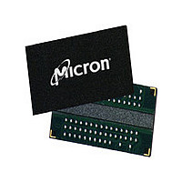
MT47H32M16HR-3 IT:F TR Micron Technology Inc, MT47H32M16HR-3 IT:F TR Datasheet - Page 79

MT47H32M16HR-3 IT:F TR
Manufacturer Part Number
MT47H32M16HR-3 IT:F TR
Description
DRAM Chip DDR2 SDRAM 512M-Bit 32Mx16 1.8V 84-Pin FBGA T/R
Manufacturer
Micron Technology Inc
Type
DDR2 SDRAMr
Specifications of MT47H32M16HR-3 IT:F TR
Density
512 Mb
Maximum Clock Rate
667 MHz
Package
84FBGA
Address Bus Width
15 Bit
Operating Supply Voltage
1.8 V
Maximum Random Access Time
0.45 ns
Operating Temperature
-40 to 85 °C
Organization
32Mx16
Address Bus
15b
Access Time (max)
450ps
Operating Supply Voltage (typ)
1.8V
Package Type
FBGA
Operating Temp Range
-40C to 85C
Operating Supply Voltage (max)
1.9V
Operating Supply Voltage (min)
1.7V
Supply Current
250mA
Pin Count
84
Mounting
Surface Mount
Operating Temperature Classification
Industrial
Lead Free Status / RoHS Status
Compliant
- Current page: 79 of 132
- Download datasheet (10Mb)
CAS Latency (CL)
Figure 35: CL
PDF: 09005aef82f1e6e2
512MbDDR2.pdf - Rev. R 12/10 EN
Notes:
The CAS latency (CL) is defined by bits M4–M6, as shown in Figure 34 (page 76). CL is
the delay, in clock cycles, between the registration of a READ command and the availa-
bility of the first bit of output data. The CL can be set to 3, 4, 5, 6, or 7 clocks, depending
on the speed grade option being used.
DDR2 SDRAM does not support any half-clock latencies. Reserved states should not be
used as an unknown operation otherwise incompatibility with future versions may result.
DDR2 SDRAM also supports a feature called posted CAS additive latency (AL). This fea-
ture allows the READ command to be issued prior to
internal command to the DDR2 SDRAM by AL clocks. The AL feature is described in
further detail in Posted CAS Additive Latency (AL) (page 82).
Examples of CL = 3 and CL = 4 are shown in Figure 35; both assume AL = 0. If a READ
command is registered at clock edge n, and the CL is m clocks, the data will be available
nominally coincident with clock edge n + m (this assumes AL = 0).
DQS, DQS#
DQS, DQS#
Command
Command
1. BL = 4.
2. Posted CAS# additive latency (AL) = 0.
3. Shown with nominal
CK#
CK#
DQ
DQ
CK
CK
READ
READ
T0
T0
NOP
NOP
T1
T1
CL = 3 (AL = 0)
t
AC,
79
t
DQSCK, and
CL = 4 (AL = 0)
NOP
NOP
T2
T2
Micron Technology, Inc. reserves the right to change products or specifications without notice.
t
DQSQ.
512Mb: x4, x8, x16 DDR2 SDRAM
NOP
NOP
T3
T3
DO
n
t
RCD (MIN) by delaying the
n + 1
DO
NOP
NOP
T4
T4
Mode Register (MR)
n + 2
DO
DO
n
© 2004 Micron Technology, Inc. All rights reserved.
Transitioning data
n + 1
n + 3
DO
DO
NOP
NOP
T5
T5
n + 2
DO
n + 3
DO
NOP
NOP
Don’t care
T6
T6
Related parts for MT47H32M16HR-3 IT:F TR
Image
Part Number
Description
Manufacturer
Datasheet
Request
R

Part Number:
Description:
IC DDR2 SDRAM 512MBIT 84FBGA
Manufacturer:
Micron Technology Inc
Datasheet:

Part Number:
Description:
IC DDR2 SDRAM 512MBIT 3NS 84FBGA
Manufacturer:
Micron Technology Inc
Datasheet:

Part Number:
Description:
32MX16 DDR2 SDRAM PLASTIC IND TEMP PBF FBGA 1.8V
Manufacturer:
Micron Technology Inc
Datasheet:

Part Number:
Description:
Manufacturer:
Micron Technology Inc
Datasheet:

Part Number:
Description:
Manufacturer:
Micron Technology Inc
Datasheet:

Part Number:
Description:
Manufacturer:
Micron Technology Inc
Datasheet:

Part Number:
Description:
Manufacturer:
Micron Technology Inc
Datasheet:

Part Number:
Description:
MICMT47H32M16HR-3_IT:F 32MBX16 DDR2
Manufacturer:
Micron Technology Inc
Datasheet:

Part Number:
Description:
Manufacturer:
Micron Technology Inc
Datasheet:

Part Number:
Description:
Manufacturer:
Micron Technology Inc
Datasheet:

Part Number:
Description:
Manufacturer:
Micron Technology Inc
Datasheet:

Part Number:
Description:
32MX16 DDR2 SDRAM PLASTIC IND TEMP PBF FBGA 1.8V
Manufacturer:
Micron Technology Inc

Part Number:
Description:
IC DDR2 SDRAM 512MBIT 84FBGA
Manufacturer:
Micron Technology Inc
Datasheet:

Part Number:
Description:
Manufacturer:
Micron Technology Inc
Datasheet:

Part Number:
Description:
Manufacturer:
Micron Technology Inc
Datasheet:


