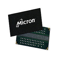
MT47H32M16HR-3 IT:F TR Micron Technology Inc, MT47H32M16HR-3 IT:F TR Datasheet - Page 29

MT47H32M16HR-3 IT:F TR
Manufacturer Part Number
MT47H32M16HR-3 IT:F TR
Description
DRAM Chip DDR2 SDRAM 512M-Bit 32Mx16 1.8V 84-Pin FBGA T/R
Manufacturer
Micron Technology Inc
Type
DDR2 SDRAMr
Specifications of MT47H32M16HR-3 IT:F TR
Density
512 Mb
Maximum Clock Rate
667 MHz
Package
84FBGA
Address Bus Width
15 Bit
Operating Supply Voltage
1.8 V
Maximum Random Access Time
0.45 ns
Operating Temperature
-40 to 85 °C
Organization
32Mx16
Address Bus
15b
Access Time (max)
450ps
Operating Supply Voltage (typ)
1.8V
Package Type
FBGA
Operating Temp Range
-40C to 85C
Operating Supply Voltage (max)
1.9V
Operating Supply Voltage (min)
1.7V
Supply Current
250mA
Pin Count
84
Mounting
Surface Mount
Operating Temperature Classification
Industrial
Lead Free Status / RoHS Status
Compliant
Table 11: DDR2 I
Notes: 1–7 apply to the entire table
PDF: 09005aef82f1e6e2
512MbDDR2.pdf - Rev. R 12/10 EN
Parameter/Condition
Operating burst write current: All
banks open, continuous burst writes;
BL = 4, CL = CL (I
(I
(I
tween valid commands; address bus
inputs are switching; Data bus inputs
are switching
Operating burst read current: All
banks open, continuous burst reads,
I
0;
t
CKE is HIGH, CS# is HIGH between val-
id commands; address bus inputs are
switching; Data bus inputs are switch-
ing
Burst refresh current:
(I
(I
HIGH between valid commands; Oth-
er control and address bus inputs are
switching; Data bus inputs are switch-
ing
Self refresh current: CK and CK# at
0V; CKE ≤ 0.2V; Other control and ad-
dress bus inputs are floating; Data
bus inputs are floating
Operating bank interleave read
current: All bank interleaving reads,
I
t
(I
(I
CS# is HIGH between valid commands;
address bus inputs are stable during
deselects; Data bus inputs are switch-
ing; See I
details
OUT
RAS =
OUT
RCD (I
DD
DD
DD
DD
DD
DD
t
CK =
),
); CKE is HIGH, CS# is HIGH be-
); refresh command at every
) interval; CKE is HIGH, CS# is
),
),
= 0mA; BL = 4, CL = CL (I
= 0mA; BL = 4, CL = CL (I
t
t
t
RAS =
RC =
RCD =
DD
t
RAS MAX (I
t
CK (I
) - 1 x
DD7
t
RC (I
t
t
Conditions (page 24) for
RAS MAX (I
DD
RCD (I
t
),
CK (I
DD
DD
), AL = 0;
),
DD
DD
DD
DD
t
RRD =
),
Notes:
); CKE is HIGH,
);
Specifications and Conditions (Die Revision G) (Continued)
t
RP =
t
t
DD
CK =
CK =
),
t
t
RRD
DD
DD
CK =
t
t
RP =
RP (I
t
t
1. I
2. V
3. I
4. Data bus consists of DQ, DM, DQS, DQS#, RDQS, RDQS#, LDQS, LDQS#, UDQS, and
), AL =
), AL =
CK
CK
t
RFC
UDQS#. I
t
DD
t
DD
DD
CK
RP
DD
);
specifications are tested after the device is properly initialized. 0°C ≤ T
parameters are specified with ODT disabled.
= +1.8V ±0.1V, V
Symbol
I
I
I
DD4W
I
I
I
DD4R
DD6L
DD5
DD6
DD7
DD
values must be met with all combinations of EMR bits 10 and 11.
Configura-
x4, x8, x16
x4, x8
x4, x8
x4, x8
x4, x8
tion
x16
x16
x16
x16
DDQ
= +1.8V ±0.1V, V
29
Electrical Specifications – I
-187E
TBD
TBD
TBD
TBD
TBD
TBD
TBD
TBD
TBD
TBD
Micron Technology, Inc. reserves the right to change products or specifications without notice.
512Mb: x4, x8, x16 DDR2 SDRAM
-25E/
DDL
125
160
120
150
100
150
215
-25
95
7
3
= +1.8V ±0.1V, V
-3E/-3
115
135
110
125
140
200
90
90
7
3
-37E
© 2004 Micron Technology, Inc. All rights reserved.
120
110
135
195
99
95
90
90
REF
7
3
= V
DD
DDQ
105
130
190
-5E
85
80
95
87
87
7
3
Parameters
/2.
C
≤ +85°C.
Units
mA
mA
mA
mA
mA


