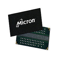
MT47H32M16HR-3 IT:F TR Micron Technology Inc, MT47H32M16HR-3 IT:F TR Datasheet - Page 77

MT47H32M16HR-3 IT:F TR
Manufacturer Part Number
MT47H32M16HR-3 IT:F TR
Description
DRAM Chip DDR2 SDRAM 512M-Bit 32Mx16 1.8V 84-Pin FBGA T/R
Manufacturer
Micron Technology Inc
Type
DDR2 SDRAMr
Specifications of MT47H32M16HR-3 IT:F TR
Density
512 Mb
Maximum Clock Rate
667 MHz
Package
84FBGA
Address Bus Width
15 Bit
Operating Supply Voltage
1.8 V
Maximum Random Access Time
0.45 ns
Operating Temperature
-40 to 85 °C
Organization
32Mx16
Address Bus
15b
Access Time (max)
450ps
Operating Supply Voltage (typ)
1.8V
Package Type
FBGA
Operating Temp Range
-40C to 85C
Operating Supply Voltage (max)
1.9V
Operating Supply Voltage (min)
1.7V
Supply Current
250mA
Pin Count
84
Mounting
Surface Mount
Operating Temperature Classification
Industrial
Lead Free Status / RoHS Status
Compliant
Burst Type
Table 41: Burst Definition
Operating Mode
DLL RESET
PDF: 09005aef82f1e6e2
512MbDDR2.pdf - Rev. R 12/10 EN
Burst Length
4
8
Starting Column Address
Accesses within a given burst may be programmed to be either sequential or inter-
leaved. The burst type is selected via bit M3, as shown in Figure 34. The ordering of
accesses within a burst is determined by the burst length, the burst type, and the start-
ing column address, as shown in Table 41. DDR2 SDRAM supports 4-bit burst mode
and 8-bit burst mode only. For 8-bit burst mode, full interleaved address ordering is
supported; however, sequential address ordering is nibble-based.
The normal operating mode is selected by issuing a command with bit M7 set to “0,”
and all other bits set to the desired values, as shown in Figure 34 (page 76). When bit M7
is “1,” no other bits of the mode register are programmed. Programming bit M7 to “1”
places the DDR2 SDRAM into a test mode that is only used by the manufacturer and
should not be used. No operation or functionality is guaranteed if M7 bit is “1.”
DLL RESET is defined by bit M8, as shown in Figure 34. Programming bit M8 to “1” will
activate the DLL RESET function. Bit M8 is self-clearing, meaning it returns back to a
value of “0” after the DLL RESET function has been issued.
Anytime the DLL RESET function is used, 200 clock cycles must occur before a READ
command can be issued to allow time for the internal clock to be synchronized with the
external clock. Failing to wait for synchronization to occur may result in a violation of
the
(A2, A1, A0)
t
AC or
0 0 0
0 0 1
0 1 0
0 1 1
1 0 0
1 0 1
1 1 0
1 1 1
0 0
0 1
1 0
1 1
t
DQSCK parameters.
Burst Type = Sequential
77
0, 1, 2, 3, 4, 5, 6, 7
1, 2, 3, 0, 5, 6, 7, 4
2, 3, 0, 1, 6, 7, 4, 5
3, 0, 1, 2, 7, 4, 5, 6
4, 5, 6, 7, 0, 1, 2, 3
5, 6, 7, 4, 1, 2, 3, 0
6, 7, 4, 5, 2, 3, 0, 1
7, 4, 5, 6, 3, 0, 1, 2
0, 1, 2, 3
1, 2, 3, 0
2, 3, 0, 1
3, 0, 1, 2
Micron Technology, Inc. reserves the right to change products or specifications without notice.
Order of Accesses Within a Burst
512Mb: x4, x8, x16 DDR2 SDRAM
Burst Type = Interleaved
Mode Register (MR)
© 2004 Micron Technology, Inc. All rights reserved.
0, 1, 2, 3, 4, 5, 6, 7
1, 0, 3, 2, 5, 4, 7, 6
2, 3, 0, 1, 6, 7, 4, 5
3, 2, 1, 0, 7, 6, 5, 4
4, 5, 6, 7, 0, 1, 2, 3
5, 4, 7, 6, 1, 0, 3, 2
6, 7, 4, 5, 2, 3, 0, 1
7, 6, 5, 4, 3, 2, 1, 0
0, 1, 2, 3
1, 0, 3, 2
2, 3, 0, 1
3, 2, 1, 0


