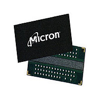
MT47H32M16HR-3 IT:F TR Micron Technology Inc, MT47H32M16HR-3 IT:F TR Datasheet - Page 118

MT47H32M16HR-3 IT:F TR
Manufacturer Part Number
MT47H32M16HR-3 IT:F TR
Description
DRAM Chip DDR2 SDRAM 512M-Bit 32Mx16 1.8V 84-Pin FBGA T/R
Manufacturer
Micron Technology Inc
Type
DDR2 SDRAMr
Specifications of MT47H32M16HR-3 IT:F TR
Density
512 Mb
Maximum Clock Rate
667 MHz
Package
84FBGA
Address Bus Width
15 Bit
Operating Supply Voltage
1.8 V
Maximum Random Access Time
0.45 ns
Operating Temperature
-40 to 85 °C
Organization
32Mx16
Address Bus
15b
Access Time (max)
450ps
Operating Supply Voltage (typ)
1.8V
Package Type
FBGA
Operating Temp Range
-40C to 85C
Operating Supply Voltage (max)
1.9V
Operating Supply Voltage (min)
1.7V
Supply Current
250mA
Pin Count
84
Mounting
Surface Mount
Operating Temperature Classification
Industrial
Lead Free Status / RoHS Status
Compliant
Table 44: Truth Table – CKE
Notes 1–4 apply to the entire table
PDF: 09005aef82f1e6e2
512MbDDR2.pdf - Rev. R 12/10 EN
Current State
Bank(s) active
All banks idle
Power-down
Self refresh
Previous Cycle
Notes:
(n - 1)
H
H
H
H
L
L
L
L
10. Valid commands for self refresh exit are NOP and DESELECT only.
11. Power-down and self refresh can not be entered while READ or WRITE operations,
12. Minimum CKE high time is
13. Self refresh mode can only be entered from the all banks idle state.
14. Must be a legal command, as defined in Table 37 (page 69).
1. CKE (n) is the logic state of CKE at clock edge n; CKE (n - 1) was the state of CKE at the
2. Current state is the state of the DDR2 SDRAM immediately prior to clock edge n.
3. Command (n) is the command registered at clock edge n, and action (n) is a result of
4. The state of ODT does not affect the states described in this table. The ODT function is
5. Power-down modes do not perform any REFRESH operations. The duration of power-
6. “X” means “Don’t Care” (including floating around V
7. All states and sequences not shown are illegal or reserved unless explicitly described else-
8. Valid commands for power-down entry and exit are NOP and DESELECT only.
9. On self refresh exit, DESELECT or NOP commands must be issued on every clock edge
previous clock edge.
command (n).
not available during self refresh (see ODT Timing (page 126) for more details and specif-
ic restrictions).
down mode is therefore limited by the refresh requirements.
down. However, ODT must be driven high or low in power-down if the ODT function is
enabled via EMR.
where in this document.
occurring during the
(200 clocks) is satisfied.
LOAD MODE operations, or PRECHARGE operations are in progress. See SELF REFRESH
(page 114) and SELF REFRESH (page 75) for a list of detailed restrictions.
This requires a minimum of 3 clock cycles of registration.
CKE
Cycle (n)
Current
H
H
H
L
L
L
L
L
t
XSNR period. READ commands may be issued only after
CS#, RAS#, CAS#,
118
DESELECT or NOP
DESELECT or NOP
DESELECT or NOP Active power-down entry
DESELECT or NOP
Command (n)
t
CKE = 3 ×
Refresh
WE#
Shown in Table 37 (page 69)
X
X
Micron Technology, Inc. reserves the right to change products or specifications without notice.
t
CK. Minimum CKE LOW time is
512Mb: x4, x8, x16 DDR2 SDRAM
Precharge power-down
Maintain power-down
Maintain self refresh
Self refresh entry
Power-down exit
Self refresh exit
Action (n)
REF
entry
) in self refresh and power-
Power-Down Mode
© 2004 Micron Technology, Inc. All rights reserved.
t
CKE = 3 ×
7, 8, 11, 12
10, 12, 13
7, 9, 10
7, 8, 11
Notes
t
5, 6
7, 8
14
XSRD
6
t
CK.


