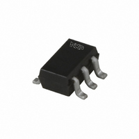
BFM520,115 NXP Semiconductors, BFM520,115 Datasheet - Page 2

BFM520,115
Manufacturer Part Number
BFM520,115
Description
TRANS NPN DUAL 70MA 8V SOT363
Manufacturer
NXP Semiconductors
Datasheet
1.BFM520115.pdf
(12 pages)
Specifications of BFM520,115
Package / Case
SC-70-6, SC-88, SOT-363
Transistor Type
2 NPN (Dual)
Voltage - Collector Emitter Breakdown (max)
8V
Frequency - Transition
9GHz
Noise Figure (db Typ @ F)
1.2dB ~ 2.1dB @ 900MHz
Power - Max
1W
Dc Current Gain (hfe) (min) @ Ic, Vce
60 @ 20mA, 6V
Current - Collector (ic) (max)
70mA
Mounting Type
Surface Mount
Dc Current Gain Hfe Max
60 @ 20mA @ 6V
Mounting Style
SMD/SMT
Configuration
Dual
Transistor Polarity
NPN
Maximum Operating Frequency
9000 MHz (Typ)
Collector- Emitter Voltage Vceo Max
8 V
Emitter- Base Voltage Vebo
2.5 V
Continuous Collector Current
0.07 A
Power Dissipation
1000 mW
Maximum Operating Temperature
+ 175 C
Lead Free Status / RoHS Status
Lead free / RoHS Compliant
Gain
-
Lead Free Status / Rohs Status
Lead free / RoHS Compliant
Other names
568-1646-2
934041410115
BFM520 T/R
934041410115
BFM520 T/R
NXP Semiconductors
FEATURES
Small size
Temperature and h
Low noise and high gain
High gain at low current and low capacitance at low
Gold metallization ensures excellent reliability.
APPLICATIONS
Oscillator and buffer amplifiers
Balanced amplifiers
LNA/mixers.
DESCRIPTION
Dual transistor with two silicon NPN RF dies in a surface
mount 6-pin SOT363 (S-mini) package. The transistor is
primarily intended for wideband applications in the
GHz-range in the RF front end of analog and digital cellular
phones, cordless phones, radar detectors, pagers and
satellite TV-tuners.
QUICK REFERENCE DATA
1996 Oct 08
Any single transistor
C
f
G
F
R
SYMBOL
T
s
voltage
Dual NPN wideband transistor
re
th j-s
UM
21
2
feedback capacitance
transition frequency
insertion power gain
maximum unilateral power gain
noise figure
thermal resistance from junction
to soldering point
FE
PARAMETER
matched
I
I
I
I
f = 900 MHz; T
f = 900 MHz; T
I
f = 900 MHz;
single loaded
double loaded
e
C
C
C
C
= 0; V
= 20 mA; V
= 20 mA; V
= 20 mA; V
= 5 mA; V
CB
2
CONDITIONS
= 3 V; f = 1 MHz
CE
PINNING - SOT363A
handbook, halfpage
CE
CE
CE
PIN
S
amb
amb
= 3 V;
1
2
3
4
5
6
Marking code: N2.
=
= 3 V; f = 900 MHz
= 3 V;
= 3 V;
= 25 C
= 25 C
opt
Top view
SYMBOL
6
1
Fig.1 Simplified outline and symbol.
b
e
b
e
c
c
1
1
2
2
2
1
2
5
4
3
base 1
emitter 1
collector 2
base 2
emitter 2
collector 1
13
MIN.
b 1
DESCRIPTION
0.4
9
14.5
15
1.2
TYP.
Product specification
e 1
c 1
b 2
1.6
230
115
BFM520
MAX.
MAM210
e 2
c 2
pF
GHz
dB
dB
dB
K/W
K/W
UNIT


