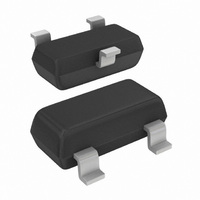
BFS17,215 NXP Semiconductors, BFS17,215 Datasheet - Page 2

BFS17,215
Manufacturer Part Number
BFS17,215
Description
TRANS NPN 25MA 15V 1GHZ SOT23
Manufacturer
NXP Semiconductors
Datasheet
1.BFS17215.pdf
(8 pages)
Specifications of BFS17,215
Package / Case
SOT-23-3, TO-236-3, Micro3™, SSD3, SST3
Transistor Type
NPN
Voltage - Collector Emitter Breakdown (max)
15V
Frequency - Transition
1GHz
Noise Figure (db Typ @ F)
4.5dB @ 500MHz
Power - Max
300mW
Dc Current Gain (hfe) (min) @ Ic, Vce
25 @ 2mA, 1V
Current - Collector (ic) (max)
25mA
Mounting Type
Surface Mount
Dc Current Gain Hfe Max
25 @ 2mA @ 1V
Mounting Style
SMD/SMT
Configuration
Single
Transistor Polarity
NPN
Maximum Operating Frequency
1600 MHz (Typ)
Collector- Emitter Voltage Vceo Max
15 V
Emitter- Base Voltage Vebo
2.5 V
Continuous Collector Current
0.025 A
Power Dissipation
300 mW
Maximum Operating Temperature
+ 150 C
Number Of Elements
1
Collector-emitter Voltage
15V
Collector-base Voltage
25V
Emitter-base Voltage
2.5V
Collector Current (dc) (max)
25mA
Dc Current Gain (min)
25
Frequency (max)
1.6GHz
Operating Temp Range
-65C to 150C
Operating Temperature Classification
Military
Mounting
Surface Mount
Pin Count
3
Package Type
TO-236AB
Lead Free Status / RoHS Status
Lead free / RoHS Compliant
Gain
-
Lead Free Status / Rohs Status
Lead free / RoHS Compliant
Other names
568-1652-2
933082771215
BFS17 T/R
933082771215
BFS17 T/R
NXP Semiconductors
DESCRIPTION
NPN transistor in a plastic SOT23 package.
APPLICATIONS
A wide range of RF applications such as:
PINNING
QUICK REFERENCED DATA
LIMITING VALUES
In accordance with the Absolute Maximum Rating System (IEC 134).
Note to the Quick reference data and the Limiting values
1. T
September 1995
V
V
I
P
f
F
V
V
V
I
I
P
T
T
SYMBOL
SYMBOL
C
T
C
CM
– Mixers and oscillators in TV tuners
– RF communications equipment.
stg
j
CBO
CEO
tot
CBO
CEO
EBO
tot
NPN 1 GHz wideband transistor
PIN
1
2
3
s
is the temperature at the soldering point of the collector pin.
base
emitter
collector
collector-base voltage
collector-emitter voltage
DC collector current
total power dissipation
transition frequency
noise figure
collector-base voltage
collector-emitter voltage
emitter-base voltage
DC collector current
peak collector current
total power dissipation
storage temperature
junction temperature
PARAMETER
PARAMETER
DESCRIPTION
open emitter
open base
up to T
I
I
T
C
C
j
= 25 mA; V
= 2 mA; V
= 25 C
s
= 70 C; note 1
open emitter
open base
open collector
up to T
CE
CE
= 5 V; R
= 5 V; f = 500 MHz; T
2
CONDITIONS
s
handbook, halfpage
= 70 C; note 1
Marking code: E1p.
CONDITIONS
S
= 50 ; f = 500 MHz;
j
= 25 C
Top view
1
Fig.1 SOT23.
3
1
4.5
65
MSB003
TYP.
MIN.
Product specification
2
25
15
25
300
25
15
2.5
25
50
300
+150
150
MAX.
MAX.
BFS17
V
V
mA
mW
GHz
dB
V
V
V
mA
mA
mW
C
C
UNIT
UNIT


