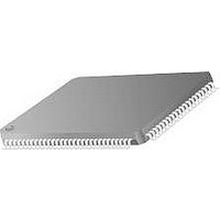
TMC2192KHC Fairchild Semiconductor, TMC2192KHC Datasheet - Page 63

TMC2192KHC
Manufacturer Part Number
TMC2192KHC
Description
Video ICs
Manufacturer
Fairchild Semiconductor
Type
Encoderr
Datasheet
1.TMC2192KHC.pdf
(69 pages)
Specifications of TMC2192KHC
Operating Supply Voltage
- 0.5 V to + 7 V
Supply Current
375 mA
Maximum Operating Temperature
70 C
Package / Case
MQFP-100
Minimum Operating Temperature
0 C
Mounting Style
SMD/SMT
Lead Free Status / RoHS Status
Lead free / RoHS Compliant
Available stocks
Company
Part Number
Manufacturer
Quantity
Price
Company:
Part Number:
TMC2192KHC
Manufacturer:
PHI
Quantity:
90
Part Number:
TMC2192KHC
Manufacturer:
FAIRCHILD/仙童
Quantity:
20 000
PRODUCT SPECIFICATION
System Performance Characteristics
Notes:
1. TTL input levels are 0.0 and 3.0 Volts, 10%-90% rise and fall times <3 ns.
2. Analog CLOAD <10 pF, D7-0 load <40 pF.
Applications Discussion
The suggested output reconstruction filter is shown in Figure
29. The phase and frequency response for the encoder and
the reconstruction filter is shown in Figure 30.
REV. 1.0.0 8/13/03
A_IN
Parameter
RES
E
E
E
dp
dg
SKEW
PSRR
100pF
LI
LD
G
-10
-20
-30
-40
C8
0
Figure 28. Typical Analog Reconstruction Filter
0
75
R8
D/A Converter Resolution
Integral Linearity Error
Differential Linearity Error
(monotonic)
Gain Error
Differential Phase
Differential Gain
CHROMA to LUMA Output
Skew
Power Supply Rejection
Ratio
R9
75
330pF
Figure 29. Overall Response
5
C7
L6
1.0 H
Frequency (MHz)
L5 1.8 H
10
27pF
C6
330pF
C7
15
D1
DIODE
SCHOTTKY
20
D2
DIODE
SCHOTTKY
65-6294-32
65-6294-31
PXCK = 27.00 MHz,40 IRE Ramp
PXCK = 27.00 MHz,40 IRE Ramp
f=1kHz
25
0
90
180
270
360
A_OUT
Conditions
The circuit in Figure 31 shows the connection of power sup-
ply voltages, output reconstruction filters and the external
voltage reference. All V
same power source.
The full-scale output voltage level for each D/A:
V
where:
• I
• R
• K is a constant for the TMC2192 D/A converters (approx-
• I
• V
• R
The reference voltage in Figure 31 is from an LM185 1.2
Volt band-gap reference. The suggested trim is designed to
give 10% of trim around 5K Ohms. This R
"gain" for that D/A converter. Varying R
cause the full-scale output voltage on the D/A to vary by
An alternative output reconstruction filter is the Microelec-
tronic Modules Corp. ST-163E, which contains 4 indepen-
dent reconstruction filter. The phase and frequency response
of this filter is shown in the Output Low-Pass Filters Section
of this data sheet.
10%.
OUTx
converter.
imately equal to 34).
pin to ground.
R
OUTx
REFx
Lx
REFx
REFx
REF
is the resistive load on the D/A output pin.
= I
= K x (V
is the voltage measured on the V
is the reference current flowing out of the R
is the full-scale output current sourced by the D/A
is the total resistance connected between the
pin and ground.
OUTx
REF
x R
Lx
/R
Min.
DD
REFx
10
= K x I
pins should be connected to the
) x R
REFx
Typ.
0.5
0.9
0.5
10
0
Lx
x R
REFx
Max.
Lx
REF
0.25
0.10
10
7.5
1
REFx
pin.
10% will
%/%V
sets the
degree
Units
TMC2192
%FS
Bits
REFx
ns
%
%
%
DD
63


