FDP3682 Fairchild Semiconductor, FDP3682 Datasheet
FDP3682
Specifications of FDP3682
Available stocks


Related parts for FDP3682


FDP3682 Summary of contents
Page 1
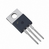
... FDB3682 / FDP3682 N-Channel PowerTrench 100V, 32A, 36m Features • 32m (Typ.), V = 10V, I DS(ON) GS • Q (tot) = 18.5nC (Typ.), V = 10V g GS • Low Miller Charge • Low Q Body Diode RR • UIS Capability (Single Pulse and Repetitive Pulse) Formerly developmental type 82755 DRAIN (FLANGE) ...
Page 2
... Source to Drain Diode Voltage SD t Reverse Recovery Time rr Q Reverse Recovery Charge RR Notes: 1: Starting T = 25° 0.27mH 20A Pulse Width = 100s ©2010 Fairchild Semiconductor Corporation FDB3682/FDP3682 Rev.B1 Package Reel Size TO-263AB 330mm TO-220AB Tube T = 25°C unless otherwise noted C Test Conditions I = 250 ...
Page 3
... SINGLE PULSE 0. Figure 3. Normalized Maximum Transient Thermal Impedance 400 TRANSCONDUCTANCE MAY LIMIT CURRENT IN THIS REGION V = 10V GS 100 ©2010 Fairchild Semiconductor Corporation FDB3682/FDP3682 Rev. 25°C unless otherwise noted 150 175 125 Figure 2. Maximum Continuous Drain Current RECTANGULAR PULSE DURATION (s) ...
Page 4
... V , GATE TO SOURCE VOLTAGE (V) GS Figure 7. Transfer Characteristics 60 PULSE DURATION = 80ms DUTY CYCLE = 0.5% MAX VGS = Id, DRAIN CURRENT (A) Figure 9. Drain to Source On Resistance vs Drain Current ©2010 Fairchild Semiconductor Corporation FDB3682/FDP3682 Rev. 25°C unless otherwise noted C 100 100 1ms 10ms 100 200 0.001 NOTE: Refer to Fairchild Application Notes AN7514 and AN7515 Figure 6 ...
Page 5
... OSS RSS GD 100 1MHz DRAIN TO SOURCE VOLTAGE (V) DS Figure 13. Capacitance vs Drain to Source Voltage ©2010 Fairchild Semiconductor Corporation FDB3682/FDP3682 Rev. 25°C unless otherwise noted C 1 250 1.1 1.0 0.9 80 120 160 200 - Figure 12. Normalized Drain to Source Breakdown Voltage vs Junction Temperature ...
Page 6
... Test Circuits and Waveforms VARY t TO OBTAIN P REQUIRED PEAK Figure 15. Unclamped Energy Test Circuit g(REF) Figure 17. Gate Charge Test Circuit Figure 19. Switching Time Test Circuit ©2010 Fairchild Semiconductor Corporation FDB3682/FDP3682 Rev. DUT 0.01 Figure 16. Unclamped Energy Waveforms DUT g(TH g(REF) 0 Figure 18. Gate Charge Waveforms ...
Page 7
... The area, in square inches or square centimeters is the top copper area including the gate and source pads. 19.84 ------------------------------------ - 26. 0.262 + Area 128 --------------------------------- - 26. 1.69 + Area ©2010 Fairchild Semiconductor Corporation FDB3682/FDP3682 Rev.B1 , and the application’s ambient never exceeded (EQ 0.1 is (0.645) DM Figure 21. Thermal Resistance vs Mounting dissipation ...
Page 8
... S2BMOD VSWITCH (RON=1e-5 ROFF=0.1 VON=0.3 VOFF=-0.4) .ENDS Note: For further discussion of the PSPICE model, consult A New PSPICE Sub-Circuit for the Power MOSFET Featuring Global Temperature Options; IEEE Power Electronics Specialist Conference Records, 1991, written by William J. Hepp and C. Frank Wheatley. ©2010 Fairchild Semiconductor Corporation FDB3682/FDP3682 Rev.B1 DPLCAP ...
Page 9
... Fairchild Semiconductor Corporation FDB3682/FDP3682 Rev.B1 DPLCAP RSLC2 - RDRAIN 6 ESG ...
Page 10
... Fairchild Semiconductor Corporation FDB3682/FDP3682 Rev.B1 JUNCTION th RTHERM1 CTHERM1 6 RTHERM2 CTHERM2 5 RTHERM3 CTHERM3 4 ...
Page 11
... Datasheet Identification Product Status Advance Information Formative / In Design Preliminary First Production No Identification Needed Full Production Obsolete Not In Production ©2010 Fairchild Semiconductor Corporation FDB3682/FDP3682 Rev.B1 ® PowerTrench ® PowerXS™ SM Programmable Active Droop™ ® QFET QS™ Quiet Series™ RapidConfigure™ ...