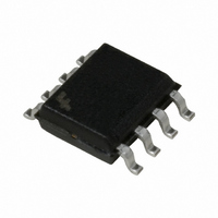
FDS6679Z Fairchild Semiconductor, FDS6679Z Datasheet - Page 4

FDS6679Z
Manufacturer Part Number
FDS6679Z
Description
MOSFET P-CH 30V 13A 8SOIC
Manufacturer
Fairchild Semiconductor
Series
PowerTrench®r
Type
Power MOSFETr
Datasheet
1.FDS6679Z.pdf
(5 pages)
Specifications of FDS6679Z
Fet Type
MOSFET P-Channel, Metal Oxide
Fet Feature
Logic Level Gate
Rds On (max) @ Id, Vgs
9 mOhm @ 13A, 10V
Drain To Source Voltage (vdss)
30V
Current - Continuous Drain (id) @ 25° C
13A
Vgs(th) (max) @ Id
3V @ 250µA
Gate Charge (qg) @ Vgs
94nC @ 10V
Input Capacitance (ciss) @ Vds
3803pF @ 15V
Power - Max
1W
Mounting Type
Surface Mount
Package / Case
8-SOIC (3.9mm Width)
Number Of Elements
1
Polarity
P
Channel Mode
Enhancement
Drain-source On-res
0.009Ohm
Drain-source On-volt
30V
Gate-source Voltage (max)
20V
Drain Current (max)
13A
Power Dissipation
2.5W
Output Power (max)
Not RequiredW
Frequency (max)
Not RequiredMHz
Noise Figure
Not RequireddB
Power Gain
Not RequireddB
Drain Efficiency
Not Required%
Operating Temp Range
-55C to 175C
Operating Temperature Classification
Military
Mounting
Surface Mount
Pin Count
8
Package Type
SOIC N
Lead Free Status / RoHS Status
Lead free / RoHS Compliant
Available stocks
Company
Part Number
Manufacturer
Quantity
Price
Company:
Part Number:
FDS6679Z
Manufacturer:
FSC
Quantity:
50 000
Company:
Part Number:
FDS6679Z
Manufacturer:
FAIRCHIL
Quantity:
70 000
Part Number:
FDS6679Z
Manufacturer:
FIR
Quantity:
20 000
Part Number:
FDS6679Z-NL
Manufacturer:
FAIRCHILD/仙童
Quantity:
20 000
Typical Characteristics
0.01
100
0.1
10
10
8
6
4
2
0
1
0.01
Figure 9. Maximum Safe Operating Area.
0
Figure 7. Gate Charge Characteristics.
0.001
0.01
SINGLE PULSE
0.1
R
R
I
0.0001
D
DS(ON)
1
JA
V
T
= -13A
GS
10
A
= 125
= 25
= -10V
LIMIT
o
o
C/W
C
0.1
-V
D = 0.5
0.2
D S
20
0.1
, DRAIN-SOURCE VOLTAGE (V)
0.05
0.02
Q
g
0.01
, GATE CHARGE (nC)
0.001
30
SINGLE PULSE
1
Figure 11. Transient Thermal Response Curve.
DC
40
Thermal characterization performed using the conditions described in Note 1c.
Transient thermal response will change depending on the circuit board design.
1s
100ms
V
DS
10ms
= -5V
50
0.01
1ms
10
100 s
-15V
60
-10V
100
70
0.1
t
1
, TIME (sec)
5000
4000
3000
2000
1000
50
40
30
20
10
0
0.001
0
Figure 8. Capacitance Characteristics.
0
C
Figure 10. Single Pulse Maximum
1
RSS
0.01
5
-V
Power Dissipation.
C
D S
OSS
, DRAIN TO SOURCE VOLTAGE (V)
0.1
10
10
t
1
, TIME (sec)
1
15
C
ISS
Duty Cycle, D = t
P(pk)
T
R
10
J
R
20
JA
100
- T
JA
(t) = r(t) + R
SINGLE PULSE
R
A
= 125
JA
= P * R
T
t
1
A
= 125°C/W
t
= 25°C
2
FDS6679Z Rev C(W)
100
25
o
C/W
f = 1 MHz
V
GS
JA
1
(t)
= 0 V
JA
/ t
2
1000
1000
30


