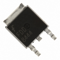
FDD8444 Fairchild Semiconductor, FDD8444 Datasheet - Page 2

FDD8444
Manufacturer Part Number
FDD8444
Description
MOSFET N-CH 40V 145A DPAK
Manufacturer
Fairchild Semiconductor
Series
PowerTrench®r
Datasheet
1.FDD8444.pdf
(7 pages)
Specifications of FDD8444
Fet Type
MOSFET N-Channel, Metal Oxide
Fet Feature
Standard
Rds On (max) @ Id, Vgs
5.2 mOhm @ 50A, 10V
Drain To Source Voltage (vdss)
40V
Current - Continuous Drain (id) @ 25° C
145A
Vgs(th) (max) @ Id
4V @ 250µA
Gate Charge (qg) @ Vgs
116nC @ 10V
Input Capacitance (ciss) @ Vds
6195pF @ 25V
Power - Max
153W
Mounting Type
Surface Mount
Package / Case
DPak, TO-252 (2 leads+tab), SC-63
Configuration
Single
Transistor Polarity
N-Channel
Resistance Drain-source Rds (on)
0.0094 Ohm @ 10 V
Drain-source Breakdown Voltage
40 V
Gate-source Breakdown Voltage
+/- 20 V
Continuous Drain Current
145 A
Power Dissipation
153000 mW
Maximum Operating Temperature
+ 175 C
Mounting Style
SMD/SMT
Minimum Operating Temperature
- 55 C
Continuous Drain Current Id
17.5A
Drain Source Voltage Vds
40V
On Resistance Rds(on)
5.2mohm
Rds(on) Test Voltage Vgs
10V
Threshold Voltage Vgs Typ
2.5V
Rohs Compliant
Yes
Lead Free Status / RoHS Status
Lead free / RoHS Compliant
Other names
FDD8444TR
Available stocks
Company
Part Number
Manufacturer
Quantity
Price
Company:
Part Number:
FDD8444
Manufacturer:
FAIRCHILD
Quantity:
30 000
Part Number:
FDD8444
Manufacturer:
FSC进口
Quantity:
20 000
Company:
Part Number:
FDD8444L
Manufacturer:
FSC
Quantity:
2 809
Part Number:
FDD8444L
Manufacturer:
FAIRCHILD/仙童
Quantity:
20 000
FDD8444 Rev B (W)
Package Marking and Ordering Information
Electrical Characteristics
Off Characteristics
On Characteristics
Dynamic Characteristics
MOSFET Maximum Ratings
Thermal Characteristics
B
I
I
V
r
C
C
C
R
Q
Q
Q
Q
Q
Q
V
V
I
E
P
T
R
R
Symbol
DSS
GSS
DS(on)
Symbol
D
J
VDSS
GS(th)
DSS
GS
AS
D
iss
oss
rss
G
θJC
θJA
Device Marking
g(TOT)
g(5)
g(TH)
gs
gs2
gd
, T
STG
FDD8444
Thermal Resistance, Junction to Case
Thermal Resistance, Junction to Ambient TO-252, 1in
Drain to Source Breakdown Voltage
Zero Gate Voltage Drain Current
Gate to Source Leakage Current
Drain to Source Voltage
Gate to Source Voltage
Drain Current Continuous (V
Continuous (V
Pulsed
Single Pulse Avalanche Energy
Power Dissipation
Derate above 25
Operating and Storage Temperature
Gate to Source Threshold Voltage
Drain to Source On Resistance
Input Capacitance
Output Capacitance
Reverse Transfer Capacitance
Gate Resistance
Total Gate Charge at 10V
Total Gate Charge at 5V
Threshold Gate Charge
Gate to Source Gate Charge
Gate Charge Threshold to Plateau
Gate to Drain “Miller“ Charge
GS
FDD8444
Parameter
Device
o
= 10V, with R
C
GS
T
θJA
= 10V)
J
Parameter
TO-252AA
= 25°C unless otherwise noted
Package
T
= 52
C
= 25°C unless otherwise noted
o
C/W)
V
f = 1MHz
f = 1MHz
V
V
V
V
I
I
T
I
V
V
V
D
D
D
J
DS
GS
GS
GS
GS
DS
GS
GS
= 250μA, V
= 50A, V
= 50A, V
= 175
= 25V, V
= 0 to 10V
= 0 to 5V
= 0 to 2V
= 32V
= V
= 0V
= ±20V
Test Conditions
DS
2
o
C
, I
Reel Size
GS
GS
D
2
GS
GS
= 10V
= 10V,
copper pad area
13”
= 250μA
= 0V
= 0V,
V
I
I
T
D
g
DD
J
= 1.0mA
= 50A
= 150
= 20V
(Note 1)
(Note 2)
o
C
Tape Width
12mm
Min
40
2
-
-
-
-
-
-
-
-
-
-
-
-
-
-
-55 to +175
Ratings
Figure 4
6195
0.98
585
332
Typ
1.02
1.9
2.5
7.2
±20
153
89
43
23
20
145
535
52
11
11
40
20
4
-
-
-
-
www.fairchildsemi.com
2500 units
±100
14.3
Quantity
Max
250
116
5.2
9.4
56
1
-
-
-
-
4
-
-
-
-
Units
o
o
Units
W/
μA
nA
mΩ
nC
nC
nC
nC
nC
nC
C/W
C/W
pF
pF
pF
Ω
mJ
V
o
W
V
V
V
A
C
o
C


