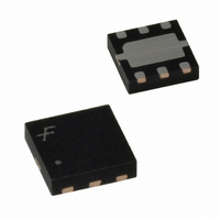
FDFM2P110 Fairchild Semiconductor, FDFM2P110 Datasheet - Page 2

FDFM2P110
Manufacturer Part Number
FDFM2P110
Description
MOSFET P-CH 20V 3.5A 3X3 MLP
Manufacturer
Fairchild Semiconductor
Series
PowerTrench®r
Datasheet
1.FDFM2P110.pdf
(7 pages)
Specifications of FDFM2P110
Fet Type
MOSFET P-Channel, Metal Oxide
Fet Feature
Diode (Isolated)
Rds On (max) @ Id, Vgs
140 mOhm @ 3.5A, 4.5V
Drain To Source Voltage (vdss)
20V
Current - Continuous Drain (id) @ 25° C
3.5A
Vgs(th) (max) @ Id
1.5V @ 250µA
Gate Charge (qg) @ Vgs
4nC @ 4.5V
Input Capacitance (ciss) @ Vds
280pF @ 10V
Power - Max
800mW
Mounting Type
Surface Mount
Package / Case
6-MLP, Power33
Configuration
Single Dual Source
Transistor Polarity
P-Channel
Resistance Drain-source Rds (on)
0.14 Ohms
Drain-source Breakdown Voltage
- 20 V
Gate-source Breakdown Voltage
+/- 12 V
Continuous Drain Current
3.5 A
Power Dissipation
2 W
Maximum Operating Temperature
+ 150 C
Mounting Style
SMD/SMT
Minimum Operating Temperature
- 55 C
Lead Free Status / RoHS Status
Lead free / RoHS Compliant
Available stocks
Company
Part Number
Manufacturer
Quantity
Price
Part Number:
FDFM2P110
Manufacturer:
FAIRCHILD/仙童
Quantity:
20 000
Electrical Characteristics
Off Characteristics
On Characteristics
Dynamic Characteristics
Switching Characteristics
Drain-Source Diode Characteristics and Maximum Ratings
Schottky Diode Characteristic
B
∆BV
∆T
I
I
V
∆V
∆T
R
I
g
C
C
C
R
t
t
t
t
Q
Q
Q
I
V
t
Q
V
I
V
DSS
GSS
D(ON)
d(ON)
r
d(OFF)
f
S
rr
R
FS
VDSS
GS(TH)
SD
R
F
DS(ON)
ISS
OSS
RSS
G
g
gs
gd
rr
Symbol
J
GS(TH)
J
DSS
Drain-Source Breakdown Voltage
Breakdown Voltage Temperature
Coefficient
Zero Gate Voltage Drain Current
Gate-Body Leakage,
Gate Threshold Voltage
Gate Threshold Voltage
Temperature Coefficient
Static Drain-Source On-Resistance
On-State Drain Current
Forward Transconductance
Input Capacitance
Output Capacitance
Reverse Transfer Capacitance
Gate Resistance
Turn-On Delay Time
Turn-On Rise Time
Turn-Off Delay Time
Turn-Off Fall Time
Total Gate Charge
Gate-Source Charge
Gate-Drain Charge
Maximum Continuous Drain-Source Diode Forward Current
Drain-Source Diode Forward Voltage
Diode Reverse Recovery Time
Diode Reverse Recovery Charge
Forward Voltage
Reverse Voltage
Reverse Leakage
(Note 2)
Parameter
(Note 2)
T
A
= 25°C unless otherwise noted
I
V
I
I
I
Referenced to 25°C
V
V
V
I
Referenced to 25°C
I
I
I
T
V
I
V
f = 1MHz
f = 1MHz
V
V
V
V
V
I
R
F
D
D
D
D
D
D
D
F
J
R
GS
GS
DS
GS
DS
DD
GS
DS
GS
GS
= -3.5A, dI
= 1A
= 1mA
= -250µA, V
= -250µA,
= -250µA,
= -3.5A, V
= -3.0A, V
= -3.5A, V
= -3.5A, V
= 125°C
= 5V
2
= V
= -10V, V
= -10V, I
= 0V, V
= ±12V, V
= -2.5V, V
= -10V, I
= -4.5V, R
= -4.5V
= 0V, I
Test Conditions
GS
, I
S
DS
F
D
GS
GS
GS
DS
= -2 A
D
D
/dt=100A/µs
GS
GS
= -250µA
DS
DS
GEN
= -3.5A,
= -16V
= -1A
= -5V
= -4.5V
= -2.5V
= -4.5V,
T
T
T
= 0V,
= 0V
= 0V
= -5V
J
J
J
= 16Ω
= 25°C
= 100°C
= 25°C
(Note 2)
20
Min
-0.6
-20
-10
-
-
-
-
-
-
-
-
-
-
-
-
-
-
-
-
-
-
-
-
-
-
-
-
-
0.32
Typ
-1.0
280
-0.9
101
145
136
-11
-
-
3.2
0.7
65
35
12
11
13
7
3
6
8
3
1
3
-
-
-
-
-
FDFM2P110 Rev. C4 (W)
0.39
100
±100
10
Max
-1.5
140
200
202
-1.2
6.4
-
-1
16
22
20
-2
4
-
-
-
-
-
-
-
-
-
-
-
-
-
mV/°C
mV/°C
Units
mA
µA
mΩ
µA
pF
pF
pF
nC
nC
nC
nC
V
V
nA
ns
ns
ns
ns
ns
Ω
V
V
A
S
A
V


