FDFM2P110 Fairchild Semiconductor, FDFM2P110 Datasheet
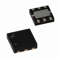
MOSFET P-CH 20V 3.5A 3X3 MLP

FDFM2P110

Manufacturer Part Number
FDFM2P110
Description
MOSFET P-CH 20V 3.5A 3X3 MLP
Manufacturer
Fairchild Semiconductor
Series
PowerTrench®r
Datasheet

Specifications of FDFM2P110

Fet Type
MOSFET P-Channel, Metal Oxide
Fet Feature
Diode (Isolated)
Rds On (max) @ Id, Vgs
140 mOhm @ 3.5A, 4.5V
Drain To Source Voltage (vdss)
20V
Current - Continuous Drain (id) @ 25° C
3.5A
Vgs(th) (max) @ Id
1.5V @ 250µA
Gate Charge (qg) @ Vgs
4nC @ 4.5V
Input Capacitance (ciss) @ Vds
280pF @ 10V
Power - Max
800mW
Mounting Type
Surface Mount
Package / Case
6-MLP, Power33
Configuration
Single Dual Source
Transistor Polarity
P-Channel
Resistance Drain-source Rds (on)
0.14 Ohms
Drain-source Breakdown Voltage
- 20 V
Gate-source Breakdown Voltage
+/- 12 V
Continuous Drain Current
3.5 A
Power Dissipation
2 W
Maximum Operating Temperature
+ 150 C
Mounting Style
SMD/SMT
Minimum Operating Temperature
- 55 C
Lead Free Status / RoHS Status
Lead free / RoHS Compliant

Available stocks

Company
Part Number
Manufacturer
Quantity
Price
Part Number:
FDFM2P110
Manufacturer:
FAIRCHILD/仙童
Quantity:
20 000
©2005 Fairchild Semiconductor Corporation
Absolute Maximum Ratings
Thermal Characteristics
Package Marking and Ordering Information
FDFM2P110
Integrated P-Channel PowerTrench
General Description
FDFM2P110 combines the exceptional performance of
Fairchild's PowerTrench MOSFET technology with a very
low forward voltage drop Schottky barrier rectifier in a
MicroFET package.
This device is designed specifically as a single package
solution for Buck Boost. It features a fast switching, low
gate charge MOSFET with very low on-state resistance.
V
V
I
V
I
P
T
R
R
D
O
J
DSS
GSS
RRM
D
θJA
θJA
Symbol
, T
Device Marking
STG
2P110
Drain-Source Voltage
Gate-Source Voltage
Drain Current -Continuous
Schottky Repetitive Peak Reverse voltage
Schottky Average Forward Current
Power dissipation (Steady State)
Operating and Storage Junction Temperature Range
Thermal Resistance, Junction-to-Ambient
TOP
-Pulsed
FDFM2P110
Device
MLP 3x3
Parameter
T
A
= 25°C unless otherwise noted
PIN 1
BOTTOM
Reel Size
A
7inch
A
C/D
1
S
®
Applications
Features
S
Buck Boost
-3.5 A, -20 V R
Low Profile - 0.8 mm maximun - in the new package
MicroFET 3x3 mm
MOSFET and Schottky Diode
D
G
Tape Width
(Note 1a)
(Note 1b)
(Note 1a)
(Note 1a)
(Note 1a)
(Note 1b)
12mm
R
DS(ON)
DS(ON)
A
S
G
= 200mΩ @ V
= 140mΩ @ V
2
3
1
-55 to +150
Ratings
±12
-3.5
145
-20
-10
0.8
20
60
2
2
3000 units
FDFM2P110 Rev. C4 (W)
GS
GS
Quantity
August 2005
= -2.5 V
= -4.5 V
6
4
5
Units
o
o
C/W
C/W
A
S
D
o
W
V
V
A
V
A
C

Related parts for FDFM2P110

FDFM2P110 Summary of contents

Page 1

... FDFM2P110 Integrated P-Channel PowerTrench General Description FDFM2P110 combines the exceptional performance of Fairchild's PowerTrench MOSFET technology with a very low forward voltage drop Schottky barrier rectifier in a MicroFET package. This device is designed specifically as a single package solution for Buck Boost. It features a fast switching, low gate charge MOSFET with very low on-state resistance ...

Page 2

... A (Note -3.5A, dI /dt=100A/µ 1mA 25° 100° 25° Min Typ Max Units - -11 - mV/°C µ ±100 - - nA -0.6 -1.0 -1 mV/°C - 101 140 - 145 200 mΩ - 136 202 - 280 - Ω 3 -0.9 -1 µA 100 - - 0.32 0.39 V FDFM2P110 Rev. C4 (W) ...

Page 3

... Pulse Test: Pulse Width < 300 µs, Duty Cycle < 2. 25°C unless otherwise noted A is guaranteed by design while R θCA o C/W when mounted on 2 pad copper 3 is determined by the θ 145 C/W whe mounted on a minimum pad copper Scale letter size paper FDFM2P110 Rev. C4 (W) ...

Page 4

... Body Diode Forward Voltage Variation with Source Current and Temperature 4 = -2.5V -3.0V -3.5V -4.0V -4. DRAIN CURRENT (A) D On-Resistance Variation with I = -1. 125 GATE TO SOURCE VOLTAGE (V) GS On-Resistance Variation with Gate-to-Source Voltage = 125 -55 C 0.4 0.6 0 BODY DIODE FORWARD VOLTAGE (V) SD FDFM2P110 Rev 1.2 ...

Page 5

... Transient thermal response will change depending on the circuit board design. 500 -10V 400 -15V 300 200 C 100 C rss Figure 8. 0.1 0.01 0.001 0.0001 0.00001 0.000001 0.5 0.6 0.7 0.8 0 Figure 10 1MHz iss oss DRAIN TO SOURCE VOLTAGE (V) DS Capacitance Characteristics 125 100 REVERSE VOLTAGE (V) R Schottky Diode Reverse Current FDFM2P110 Rev ...

Page 6

... FDFM2P110 Rev. C4 (W) ...

Page 7

... The datasheet is printed for reference information only. 7 SPM™ Stealth™ SuperFET™ SuperSOT™-3 SuperSOT™-6 ® SuperSOT™-8 ® SyncFET™ ® TinyLogic TINYOPTO™ TruTranslation™ UHC™ ® UltraFET UniFET™ ® VCX™ Wire™ Definition Rev. I16 FDFM2P110 Rev. C4 (W) ...

Related keywords