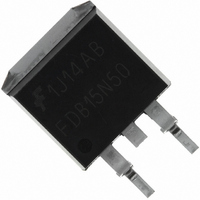
FDB15N50 Fairchild Semiconductor, FDB15N50 Datasheet

MOSFET N-CH 500V 15A TO-263AB

FDB15N50

Manufacturer Part Number
FDB15N50
Description
MOSFET N-CH 500V 15A TO-263AB
Manufacturer
Fairchild Semiconductor
Datasheet

Specifications of FDB15N50

Fet Type
MOSFET N-Channel, Metal Oxide
Fet Feature
Standard
Rds On (max) @ Id, Vgs
380 mOhm @ 7.5A, 10V
Drain To Source Voltage (vdss)
500V
Current - Continuous Drain (id) @ 25° C
15A
Vgs(th) (max) @ Id
4V @ 250µA
Gate Charge (qg) @ Vgs
41nC @ 10V
Input Capacitance (ciss) @ Vds
1850pF @ 25V
Power - Max
300W
Mounting Type
Surface Mount
Package / Case
D²Pak, TO-263 (2 leads + tab)
Configuration
Single
Transistor Polarity
N-Channel
Resistance Drain-source Rds (on)
0.3 Ohms @ 10 V
Forward Transconductance Gfs (max / Min)
10 S
Drain-source Breakdown Voltage
500 V
Gate-source Breakdown Voltage
+/- 30 V
Continuous Drain Current
15 A
Power Dissipation
300 W
Maximum Operating Temperature
+ 175 C
Mounting Style
SMD/SMT
Minimum Operating Temperature
- 55 C
Lead Free Status / RoHS Status
Lead free / RoHS Compliant
Other names
FDB15N50
FDB15N50TR

Available stocks

Company
Part Number
Manufacturer
Quantity
Price
Part Number:
FDB15N50
Manufacturer:
FAIRCHILD
Quantity:
12 500
Part Number:
FDB15N50
Manufacturer:
FAIRCHILD/仙童
Quantity:
20 000
Company:
Part Number:
FDB15N50
Quantity:
5 000
©2003 Fairchild Semiconductor Corporation
(BOTTOM)
FDH15N50 / FDP15N50 / FDB15N50
15A, 500V, 0.38 Ohm, N-Channel SMPS Power MOSFET
Applications
Switch Mode Power Supplies(SMPS), such as
• PFC Boost
• Two-Switch Forward Converter
• Single Switch Forward Converter
• Flyback Converter
• Buck Converter
• High Speed Switching
Absolute Maximum Ratings
Thermal Characteristics
Package
DRAIN
T
Symbol
R
R
R
J
V
, T
V
P
DSS
I
GS
D
JC
JA
JA
D
STG
FDH SERIES
TO-247
Thermal Resistance Junction to Case
Thermal Resistance Junction to Ambient (TO-247)
Thermal Resistance Junction to Ambient (TO-220, TO-263)
Drain to Source Voltage
Gate to Source Voltage
Drain Current
Continuous (T
Continuous (T
Pulsed
Power dissipation
Derate above 25
Operating and Storage Temperature
Soldering Temperature for 10 seconds
SOURCE
1
DRAIN
GATE
C
C
= 25
= 100
o
C
SOURCE
Parameter
o
GATE
C, V
o
C, V
GS
TO-263AB
FDB SERIES
GS
= 10V)
T
= 10V)
C
= 25
o
C unless otherwise noted
(FLANGE)
DRAIN
Features
• Low Gate Charge Q
• Improved Gate, Avalanche and High Reapplied dv/dt
• Reduced r
• Reduced Miller Capacitance and Low Input Capacitance
• Improved Switching Speed with Low EMI
• 175°C Rated Junction Temperature
Requirement
Ruggedness
(FLANGE)
DRAIN
300 (1.6mm from case)
DS(ON)
TO-220AB
FDP SERIES
-55 to 175
Ratings
±30
500
300
15
11
60
2
g
results in Simple Drive
GATE
DRAIN
FDH15N50 / FDP15N50 / FDB15N50 RevD2
SOURCE
0.50
40
62
August 2003
G
Symbol
Units
W/
o
o
D
S
W
V
V
A
A
A
C
C
o
o
o
o
C
C/W
C/W
C/W

Related parts for FDB15N50

FDB15N50 Summary of contents

Page 1

... TO-263AB FDB SERIES unless otherwise noted C Parameter 10V 10V) GS August 2003 results in Simple Drive g DS(ON) Symbol SOURCE DRAIN GATE TO-220AB FDP SERIES Ratings Units 500 V ± 300 -55 to 175 o 300 (1.6mm from case) 0. FDH15N50 / FDP15N50 / FDB15N50 RevD2 C/W o C/W o C/W ...

Page 2

... 15A, di /dt = 100A/µ Tape Width Quantity - 24mm 800 Min Typ Max 500 - - - 0. 0.33 0.38 2.0 3.4 4 150 250 - - ±100 7 5 1850 - - 230 - - 16 - 760 - - - - 0.86 1.2 - 470 730 - 5 6.6 FDH15N50 / FDP15N50 / FDB15N50 RevD2 Units V V/°C V µ µC ...

Page 3

... C 9 OSS RSS 0 100 0 Figure 6. Gate Charge Waveforms For Constant o C PULSE DURATION = 80µs DUTY CYCLE = 0.5% MAX DRAIN TO SOURCE VOLTAGE ( 10V 7. - 100 125 o TJ, JUNCTION TEMPERATURE ( C) 100V 250V 400V Qg, GATE CHARGE (nC) Gate Current FDH15N50 / FDP15N50 / FDB15N50 RevD2 100 150 175 50 ...

Page 4

... C) Figure 10. Unclamped Inductive Switching - RECTANGULAR PULSE DURATION ( 100µs 1ms 10ms DS(ON) 10 100 V , DRAIN TO SOURCE VOLTAGE (V) DS )/(1.3*RATED DSS DD *R)/(1.3*RATED +1] AS DSS DD o STARTING STARTING T = 150 TIME IN AVALANCHE (ms) AV Capability DUTY FACTOR PEAK FDH15N50 / FDP15N50 / FDB15N50 RevD2 1000 ...

Page 5

... Figure 16. Switching Time Test Circuit ©2003 Fairchild Semiconductor Corporation DUT 0.01 Figure 13. Unclamped Energy Waveforms DUT g(REF) 0 Figure 15. Gate Charge Waveforms d(ON 90 DUT V GS 50% 10% 0 Figure 17. Switching Time Waveform BV DSS g(TOT g(TH OFF t d(OFF 10% 10% 90% 50% PULSE WIDTH FDH15N50 / FDP15N50 / FDB15N50 RevD2 10V 90% ...

Page 6

... TRADEMARKS The following are registered and unregistered trademarks Fairchild Semiconductor owns or is authorized to use and is not intended exhaustive list of all such trademarks. ACEx™ FACT™ ActiveArray™ FACT Quiet Series™ ® Bottomless™ FAST CoolFET™ FASTr™ CROSSVOLT™ ...

Related keywords