FDH44N50 Fairchild Semiconductor, FDH44N50 Datasheet
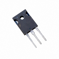
MOSFET N-CH 500V 44A TO-247

FDH44N50

Manufacturer Part Number
FDH44N50
Description
MOSFET N-CH 500V 44A TO-247
Manufacturer
Fairchild Semiconductor
Datasheet

Specifications of FDH44N50

Fet Type
MOSFET N-Channel, Metal Oxide
Fet Feature
Standard
Rds On (max) @ Id, Vgs
120 mOhm @ 22A, 10V
Drain To Source Voltage (vdss)
500V
Current - Continuous Drain (id) @ 25° C
44A
Vgs(th) (max) @ Id
4V @ 250µA
Gate Charge (qg) @ Vgs
108nC @ 10V
Input Capacitance (ciss) @ Vds
5335pF @ 25V
Power - Max
750W
Mounting Type
Through Hole
Package / Case
TO-247-3
Configuration
Single
Transistor Polarity
N-Channel
Resistance Drain-source Rds (on)
0.12 Ohm @ 10 V
Forward Transconductance Gfs (max / Min)
11 S
Drain-source Breakdown Voltage
500 V
Gate-source Breakdown Voltage
+/- 30 V
Continuous Drain Current
44 A
Power Dissipation
750000 mW
Maximum Operating Temperature
+ 175 C
Mounting Style
Through Hole
Minimum Operating Temperature
- 55 C
Lead Free Status / RoHS Status
Lead free / RoHS Compliant

Available stocks

Company
Part Number
Manufacturer
Quantity
Price
Part Number:
FDH44N50
Manufacturer:
FSC
Quantity:
4 500
Part Number:
FDH44N50
Manufacturer:
APEC
Quantity:
5 000
Part Number:
FDH44N50
Manufacturer:
FAIRCHILD/仙童
Quantity:
20 000
©2002 Fairchild Semiconductor Corporation
FDH44N50
44A, 500V, 0.12 Ohm, N-Channel SMPS Power MOSFET
Applications
Switch Mode Power Supplies(SMPS), such as
• PFC Boost
• Two-Switch Forward Converter
• Single Switch Forward Converter
• Flyback Converter
• Buck Converter
• High Speed Switching
Absolute Maximum Ratings
Thermal Characteristics
Package
(FLANGE)
T
DRAIN
Symbol
R
R
R
J
V
V
, T
P
DSS
I
GS
CS
D
JC
JA
D
STG
Thermal Resistance Junction to Case
Thermal Resistance Case to Sink, Flat, Greased Surface
Thermal Resistance Junction to Ambient
Drain to Source Voltage
Gate to Source Voltage
Drain Current
Power dissipation
Derate above 25
Operating and Storage Temperature
Soldering Temperature for 10 seconds
Mounting Torque, 8-32 or M3 Screw
Continuous (T
Continuous (T
Pulsed
JEDEC TO-247
1
C
C
o
C
= 100
= 25
Parameter
o
o
C, V
SOURCE
C, V
GS
DRAIN
GS
T
C
= 10V)
GATE
= 10V)
= 25
o
C unless otherwise noted
Features
• Low Gate Charge Q
• Improved Gate, Avalanche and High Reapplied dv/dt
• Reduced r
• Reduced Miller Capacitance and Low Input Capacitance
• Improved Switching Speed with Low EMI
• 175°C Rated Junction Temperature
Requirement
Ruggedness
300 (1.6mm from case)
DS(ON)
10ibf*in (1.1N*m)
-55 to 175
Ratings
500
176
750
44
32
G
30
5
Symbol
g
D
S
results in Simple Drive
0.24
0.2
40
FDH44N50 Rev. A4, August 2002
August 2002
Units
W/
o
o
W
V
V
A
A
A
C
C
o
o
o
o
C
C/W
C/W
C/W

Related parts for FDH44N50

FDH44N50 Summary of contents

Page 1

... Rated Junction Temperature SOURCE DRAIN GATE unless otherwise noted C Parameter 10V 10V) GS August 2002 results in Simple Drive g DS(ON) Symbol Ratings Units 500 176 A 750 -55 to 175 o 300 (1.6mm from case) 10ibf*in (1.1N*m) 0.2 0.24 40 FDH44N50 Rev. A4, August 2002 C/W o C/W o C/W ...

Page 2

... I = 44A 44A, dI /dt = 100A 44A, dI /dt = 100A Tape Width Quantity - - 30 Min Typ Max 500 - - - 0. 0.11 0. 150 250 - - ±100 108 - 5335 - - 645 - - 40 - 1500 - - - - 176 S - 0.900 1.2 - 920 1100 - 14 18 FDH44N50 Rev. A4, August 2002 Units V V/° ...

Page 3

... Figure 6. Gate Charge Waveforms For Constant o C PULSE DURATION = 80 s DUTY CYCLE = 0.5% MAX 10 VDS, DRAIN TO SOURCE VOLTAGE (V) VGS = 10V 22A - 100 125 o TJ, JUNCTION TEMPERATURE ( C) 100V 250V 400V 100 125 Qg, GATE CHARGE (nC) Gate Current FDH44N50 Rev. A4, August 2002 100 150 175 150 ...

Page 4

... Figure 8. Maximum Safe Operating Area 100 125 TC, CASE TEMPERATURE (° t1, RECTANGULAR PULSE DURATION (S) OPERATION IN THIS AREA LIMITED BY RDS(ON 100 VDS, DRAIN TO SOURCE VOLTAGE (V) 150 175 DUTY FACTOR PEAK FDH44N50 Rev. A4, August 2002 100µs 1ms 10ms DC 1000 0 10 ...

Page 5

... Figure 15. Switching Time Test Circuit ©2002 Fairchild Semiconductor Corporation DUT 0.01 Figure 12. Unclamped Energy Waveforms DUT g(REF) 0 Figure 14. Gate Charge Waveforms d(ON 90 DUT V GS 50% 10% 0 Figure 16. Switching Time Waveform BV DSS g(TOT g(TH OFF t d(OFF 10% 10% 90% 50% PULSE WIDTH FDH44N50 Rev. A4, August 2002 10V 90% ...

Page 6

CROSSVOLT â â â â ...

Related keywords